FDL100N50F
FDL100N50F is N-Channel MOSFET manufactured by Fairchild Semiconductor.
Features
- RDS(on) = 0.043Ω ( Typ.)@ VGS = 10V, ID = 50A
- Low gate charge ( Typ. 238n C)
- Low Crss ( Typ. 64p F)
- Fast switching
- 100% avalanche tested
- Improved dv/dt capability
- Ro HS pliant
Uni FETTM
May 2009
Description
These N-Channel enhancement mode power field effect transistors are produced using Fairchild’s proprietary, planar stripe, DMOS technology. This advanced technology has been especially tailored to minimize on-state resistance, provide superior switching performance, and withstand high energy pulse in the avalanche and mutation mode. These devices are well suited for high efficient switched mode power supplies and active power factor correction.
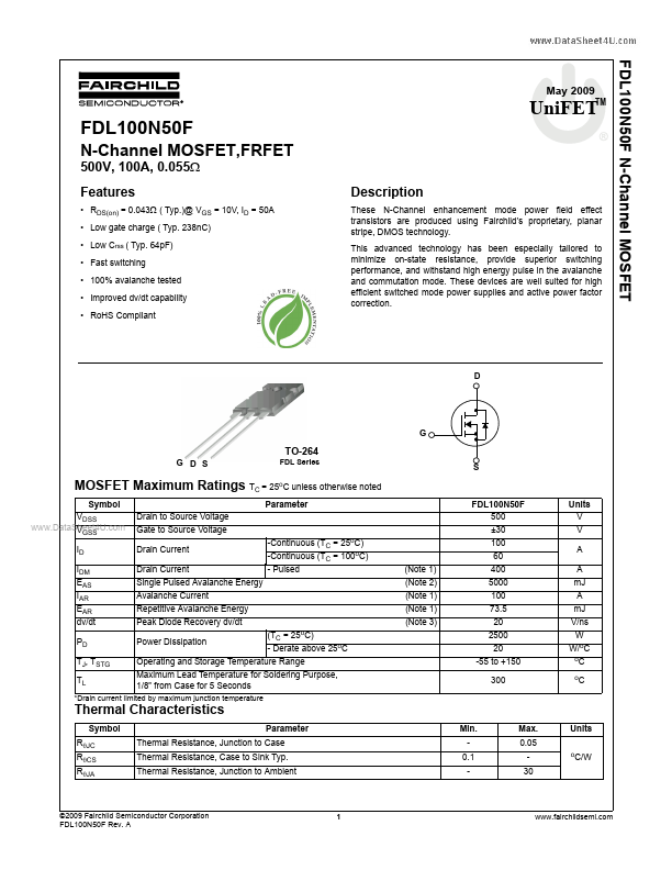
TO-264
FDL Series o
MOSFET Maximum Ratings TC = 25 C unless otherwise noted
Symbol VDSS .. V
Parameter Drain to Source Voltage Gate to Source Voltage Drain Current Drain Current Single Pulsed Avalanche Energy Avalanche Current Repetitive Avalanche Energy Peak Diode Recovery dv/dt Power Dissipation
- Derate above 25o C (TC = 25o C) -Continuous (TC = 25o C)
- Pulsed -Continuous (TC = 100o C) (Note 1) (Note 2) (Note 1) (Note 1) (Note 3)
FDL100N50F 500 ±30 100 60 400 5000 100 73.5 20 2500 20 -55 to +150 300
Units V V A A m J A m J V/ns W W/o C o o
ID IDM EAS IAR EAR dv/dt PD TJ, TSTG TL
Operating and Storage Temperature Range Maximum Lead Temperature for Soldering Purpose, 1/8” from Case for 5 Seconds
- Drain current limited by maximum junction temperature
Thermal Characteristics
Symbol RθJC RθCS RθJA Parameter Thermal Resistance, Junction to Case Thermal Resistance, Case to Sink Typ. Thermal Resistance, Junction to Ambient Min. 0.1 Max. 0.05 30 o
Units C/W
©2009 Fairchild Semiconductor Corporation FDL100N50F Rev. A
.fairchildsemi.
FDL100N50F N-Channel MOSFET
Package Marking and Ordering Information
Device Marking FDL100N50F Device FDL100N50F Package TO-264 Reel Size Tape Width Quantity 30
Electrical Characteristics TC = 25o C unless otherwise...