FDMA3023PZ
Features
General Description
This device is designed specifically as a single package solution for the battery charge switch in cellular handset and other ultra-portable applications. It features two independent P-Channel MOSFETs with low on-state resistance for minimum conduction losses. When connected in the typical mon source configuration, bi-directional current flow is possible. The Micro FET 2X2 package offers exceptional thermal performance for its physical size and is well suited to linear mode applications. tm
- Max r DS(on) = 90 mΩ at VGS = -4.5 V, ID = -2.9 A
- Max r DS(on) = 130 mΩ at VGS = -2.5 V, ID = -2.6 A
- Max r DS(on) = 170 mΩ at VGS = -1.8 V, ID = -1.7 A
- Max r DS(on) = 240 mΩ at VGS = -1.5 V, ID = -1.0 A
- Low profile
- 0.8 mm maximum
- in the new package Micro FET 2x2 mm
- HBM ESD protection level > 2 k V (Note 3)
- Ro HS pliant
- Free from halogenated pounds and antimony oxides
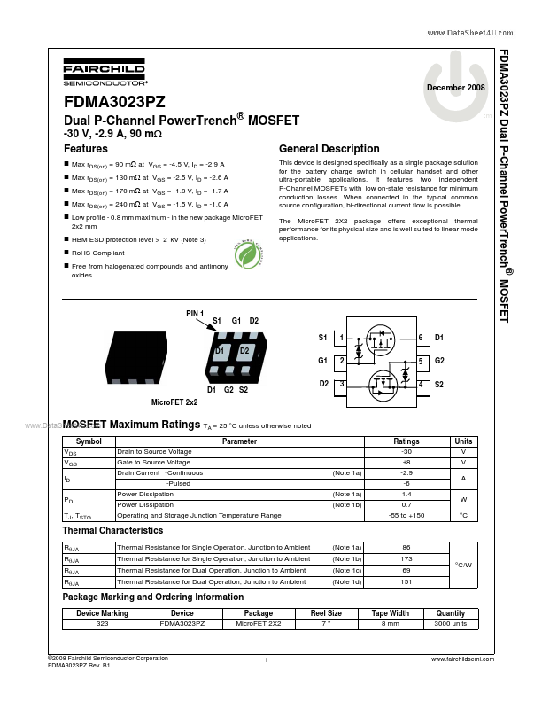
PIN 1 S1 G1 D2 S1 D1 D2 G1 D2 2 2 5 1 1 66 D1 G2 S2
5 4
D1 Micro FET 2x2
G2...