Datasheet4U.com
🌙
FDMA3027PZ Datasheet | Fairchild Semiconductor
Part:
FDMA3027PZ
Description:
MOSFET
Category:
MOSFET
Manufacturer:
Fairchild Semiconductor
Size:
488.66 KB
Download FDMA3027PZ Datasheet PDF
Related FDMA3027PZ Datasheets
FDMA3023PZ N-Channel MOSFET
FDMA3028N Dual N-Channel PowerTrench MOSFET
Fairchild Semiconductor
FDMA3027PZ
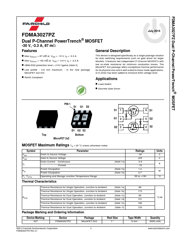
Key Features
General Description
Applications
Load Switch Discrete Gate Driver
×
Close