FDP24AN06LA0
FDP24AN06LA0 is N-Channel MOSFET manufactured by Fairchild Semiconductor.
Features
- r DS(ON) = 20mΩ (Typ.), VGS = 5V, ID = 36A
- Qg(tot) = 16n C (Typ.), VGS = 5V
- Low Miller Charge
- Low QRR Body Diode
- UIS Capability (Single Pulse and Repetitive Pulse)
- Qualified to AEC Q101
Formerly developmental type 83547
Applications
- Motor / Body Load Control
- ABS Systems
- Powertrain Management
- Injection Systems
- DC-DC converters and Off-line UPS
- Distributed Power Architectures and VRMs
- Primary Switch for 12V and 24V systems
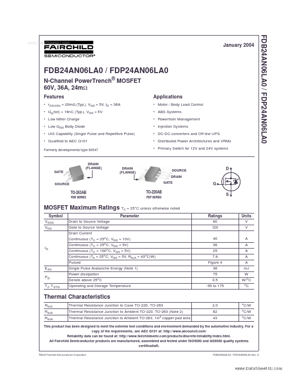
DRAIN (FLANGE) GATE
DRAIN (FLANGE)
SOURCE DRAIN
SOURCE
GATE
TO-263AB
FDB SERIES
TO-220AB
FDP SERIES
MOSFET Maximum Ratings TC = 25°C unless otherwise noted
Symbol VDSS VGS Parameter Drain to Source Voltage Gate to Source Voltage Drain Current Continuous (TC = 25o C, VGS = 10V) ID Continuous (TC = 25o C, VGS = 5V) Continuous (TC = 100o C, VGS = 5V) Continuous (TA = 25o C, VGS = 5V, Rθ JA = 43o C/W) Pulsed EAS PD TJ, TSTG Single Pulse Avalanche Energy (Note 1) Power dissipation Derate above 25o C Operating and Storage Temperature 40 36 25 7.8 Figure 4 36 75 0.5 -55 to 175 A A A A A m J W W/o C o
Ratings 60 ±20
Units V V
Thermal Characteristics
Rθ JC Rθ JA Rθ JA Thermal Resistance Junction to Case TO-220, TO-263 Thermal Resistance Junction to Ambient TO-220, TO-263 (Note 2) Thermal Resistance Junction to Ambient TO-263, 1in2 copper pad area 2.0 62 43 o C/W o o
C/W C/W
This product has been designed to meet the extreme test conditions and environment demanded by the automotive industry. For a copy of the requirements, see AEC Q101 at: http://.aecouncil./ Reliability data can be found at: http://.fairchildsemi./products/discrete/reliability/index.html. All Fairchild Semiconductor products are manufactured, assembled and tested under ISO9000 and QS9000 quality systems certification.
©2004 Fairchild Semiconductor Corporation FDB24AN06LA0 / FDP24AN06LA0 Rev. A
FDB24AN06LA0 / FDP24AN06LA0
Package .D a t a S h e Marking e t 4 U . c o and m
Device Marking FDB24AN06LA0...