Datasheet4U Logo Datasheet4U.com

FDS6064N3 Datasheet N-channel MOSFET

Manufacturer: Fairchild (now onsemi)

Overview: FDS6064N3 May 2003 FDS6064N3 20V N-Channel PowerTrench MOSFET General.

General Description

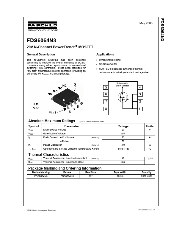
This N-Channel MOSFET has been designed specifically to improve the overall efficiency of DC/DC converters using either synchronous or conventional switching PWM controllers.

It has been optimized for “low side” synchronous rectifier operation, providing an extremely low RDS(ON) in a small package.

Applications • Synchronous rectifier • DC/DC converter • FLMP SO-8 package: Enhanced thermal performance in industry-standard package size 5 6 7 8 Bottom-side Drain Contact 4 3 2 1 Absolute Maximum Ratings Symbol VDSS VGSS ID PD TJ, TSTG Drain-Source Voltage Gate-Source Voltage Drain Current – Continuous – Pulsed Power Dissipation TA=25oC unless otherwise noted Parameter Ratings 20 ±8 (Note 1a) Units V A W °C 23 60 3.0 –55 to +150 (Note 1a) Operating and Storage Junction Temperature Range Thermal Characteristics RθJA RθJC Thermal Resistance, Junction-to-Ambient Thermal Resistance, Junction-to-Case (Note 1a) 40 0.5 °C/W Package Marking and Ordering Information Device Marking FDS6064N3 Device FDS6064N3 Reel Size 13’’ Tape width 12mm Quantity 2500 units 2002 Fairchild Semiconductor Corporation FDS6064N3 Rev B2 (W) FDS6064N3 Electrical Characteristics Symbol BVDSS ∆BVDSS ∆TJ IDSS IGSSF IGSSR VGS(th) ∆VGS(th) ∆TJ RDS(on) TA = 25°C unless otherwise noted Parameter Drain–Source Breakdown Voltage Breakdown Voltage Temperature Coefficient Zero Gate Voltage Drain Current Gate–Body Leakage, Forward Gate–Body Leakage, Reverse (Note 2) Test Conditions ID = 250 µA VGS = 0 V, ID = 250 µA, Referenced to 25°C VDS = 16 V, VGS = 8 V, VGS = –8 V , VGS = 0 V VDS = 0 V VDS = 0 V Min 20 Typ Max Units V Off Characteristics 11 1 100 –100 0.4 0.6 –3 3.4 3.8 4.9 4.5 179 7191 1403 703 VGS = 15 mV, (Note 2) mV/°C µA nA nA V mV/°C 4 5 7 8 mΩ On Characteristics Gate Threshold Voltage Gate Threshold Voltage Temperature Coefficient Static Drain–Source On–Resistance ID = 250 µA VDS = VGS, I

FDS6064N3 Distributor