FDS6690
FDS6690 is Single N-Channel Logic Level PWM Optimized PowerTrench MOSFET manufactured by Fairchild Semiconductor.
Description
This N Channel Logic Level MOSFET has been designed specifically to improve the overall efficiency of DC/DC converters using either synchronous or conventional switching PWM controllers. The MOSFET features faster switching and lower gate charge than other MOSFETs with parable RDS(ON) specifications. The result is a MOSFET that is easy and safer to drive (even at very high frequencies), and DC/DC power supply designs with higher overall efficiency.
Features
10 A, 30 V. RDS(ON) = 0.0135 Ω @ VGS = 10 V RDS(ON) = 0.0200 Ω @ VGS = 4.5 V.
Optimized for use in switching DC/DC converters with PWM controllers. Very fast switching . Low gate charge (Qg typ = 13 n C).
SOT-23
Super SOTTM-6
Super SOTTM-8
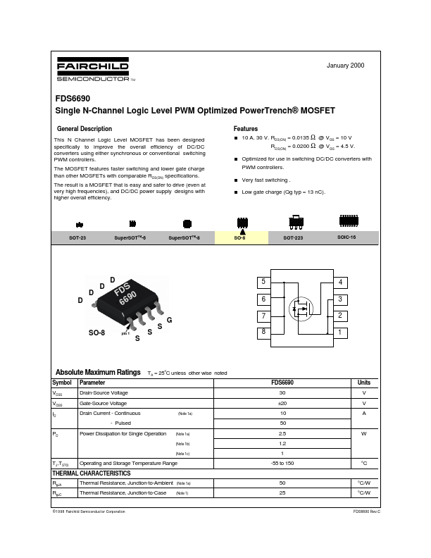
SO-8
SOT-223
SOIC-16
S FD 9 0 66
5 6 7 8
4 3 2 1
SO-8 pin 1
Absolute Maximum Ratings
Symbol VDSS VGSS ID PD Parameter Drain-Source Voltage Gate-Source Voltage Drain Current
- Continuous
- Pulsed
TA = 25o C unless other wise noted FDS6690 30 ±20
(Note 1a)
Units V V A
10 50
Power Dissipation for Single Operation
(Note 1a) (Note 1b) (Note 1c)
2.5 1.2 1 -55 to 150
TJ,TSTG RθJA RθJC
Operating and Storage Temperature Range
°C
THERMAL CHARACTERISTICS Thermal Resistance, Junction-to-Ambient Thermal Resistance, Junction-to-Case
(Note 1a) (Note 1)
50 25
°C/W °C/W
© 1998 Fairchild Semiconductor Corporation
FDS6690...