FDS6900AS
Overview
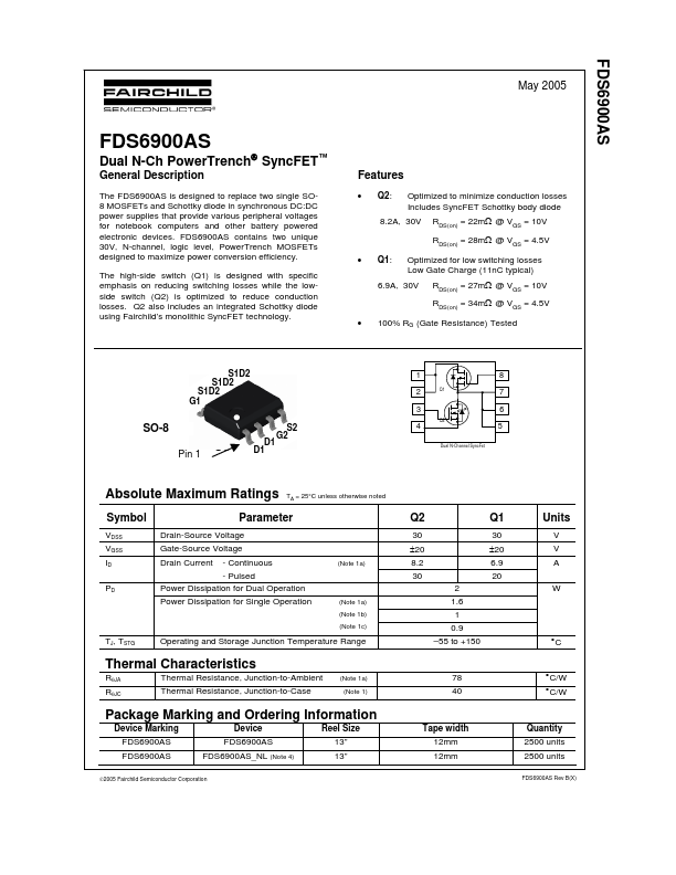
Dual N-Ch PowerTrench® SyncFET™.
- Q2: Optimized to minimize conduction losses Includes SyncFET Schottky body diode RDS(on) = 22mΩ @ VGS = 10V RDS(on) = 28mΩ @ VGS = 4.5V
- Q1: Optimized for low switching losses Low Gate Charge (11nC typical) RDS(on) = 27mΩ @ VGS = 10V RDS(on) = 34mΩ @ VGS = 4.5V
- 100% RG (Gate Resistance) Tested The FDS6900AS is designed to replace two single SO8 MOSFETs and Schottky diode in synchronous DC:DC power supplies that provide various peripheral voltages for notebook computers and other battery powered electronic devices. FDS6900AS contains two unique 30V, N-channel, logic level, PowerTrench MOSFETs designed to maximize power conversion efficiency. The high-side switch (Q1) is designed with specific emphasis on reducing switching losses while the lowside switch (Q2) is optimized to reduce conduction losses. Q2 also includes an integrated Schottky diode using Fairchild’s monolithic SyncFET technology.
- 2A, 30V
- 9A, 30V S1D2
- 1 2 3 Q2 Q1 8 7 6 5 Dual N-Channel SyncFet SO-8 Pin 1 SO- D1 D1 S S2 G2 G 4 S S