FDS6900S
Overview
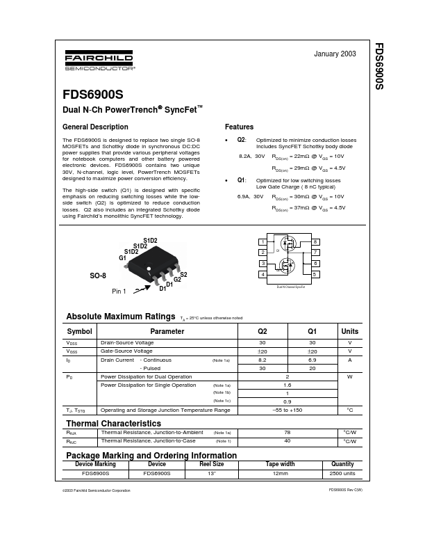
The FDS6900S is designed to replace two single SO-8 MOSFETs and Schottky diode in synchronous DC:DC power supplies that provide various peripheral voltages for notebook computers and other battery powered electronic devices. FDS6900S contains two unique 30V, N-channel, logic level, PowerTrench MOSFETs designed to maximize power conversion efficiency.
- Q2: Optimized to minimize conduction losses Includes SyncFET Schottky body diode RDS(on) = 22mΩ @ VGS = 10V RDS(on) = 29mΩ @ VGS = 4.5V
- Q1: Optimized for low switching losses Low Gate Charge ( 8 nC typical) RDS(on) = 30mΩ @ VGS = 10V RDS(on) = 37mΩ @ VGS = 4.5V
- 2A, 30V
- 9A, 30V S1D2
- 1 2 3 Q2 Q1 8 7 6 5 Dual N-Channel SyncFet SO-8 Pin 1 SO-