FOD3184
FOD3184 is High Speed MOSFET/IGBT Gate Driver Optocoupler manufactured by Fairchild Semiconductor.
Features
- High noise immunity characterized by 50k V/µs (Typ.) mon mode rejection @ VCM = 2,000V
- Guaranteed operating temperature range of -40°C to +100°C
- 3A peak output current for medium power MOSFET/IGBT
- Fast switching speed
- 210ns max. propagation delay
- 65ns max pulse width distortion
- Fast output rise/fall time
- Offers lower dynamic power dissipation
- 250k Hz maximum switching speed
- Wide VDD operating range from 15V to 30V
- Use of P-Channel MOSFETs at output stage enables output voltage swing close to the supply rail (rail-to-rail output)
- Under voltage lockout protection (UVLO) with hysteresis
- optimized for driving IGBTs
- Safety and regulatory approvals
- UL1577, 5,000 VACRMS for 1 min.
- DIN EN/IEC 60747-5-2, 1,414 peak working insulation voltage
- Minimum creepage distance of 8.0mm
- Minimum clearance distance of 8mm to 16mm
(option TV or TSV)
- Minimum insulation thickness of 0.5mm
Applications
- Plasma Display Panel
- High performance DC/DC convertor
- High performance switch mode power supply
- High performance uninterruptible power supply
- Isolated Power MOSFET/IGBT gate drive
Description
The FOD3184 is a 3A Output Current, High Speed MOSFET/IGBT Gate Drive Optocoupler. It consists of a aluminium gallium arsenide (Al Ga As) light emitting diode optically coupled to a CMOS detector with PMOS and NMOS output power transistors integrated circuit power stage. It is ideally suited for high frequency driving of power MOSFETS/IGBT used in Plasma Display Panels (PDPs), motor control inverter applications and high performance DC/DC converters.
The device is packaged in an 8-pin dual in-line housing patible with 260°C reflow processes for lead free solder pliance.
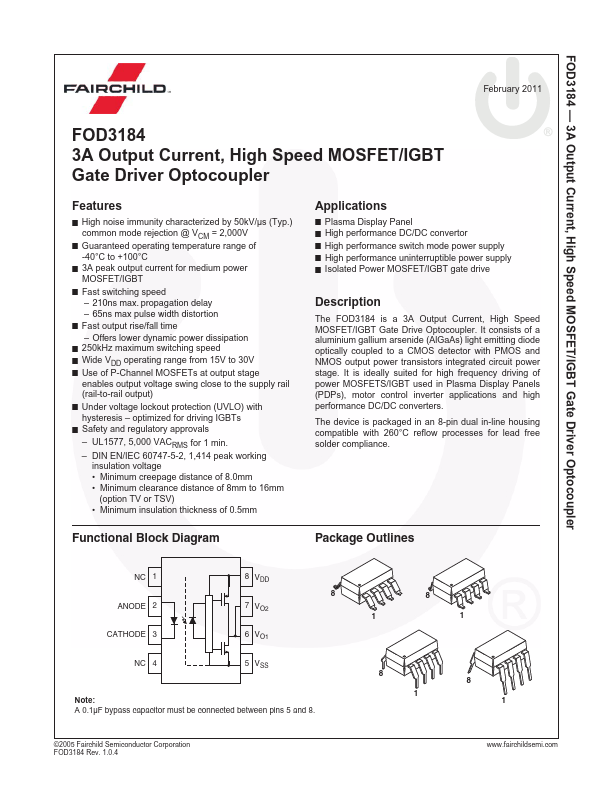
Functional Block Diagram
Package Outlines
NC 1 ANODE 2 CATHODE 3
NC 4
8 VDD 8
7 VO2
6 VO1
5 VSS
Note: A 0.1µF bypass capacitor must be connected between pins 5 and 8.
©2005 Fairchild Semiconductor Corporation FOD3184 Rev....