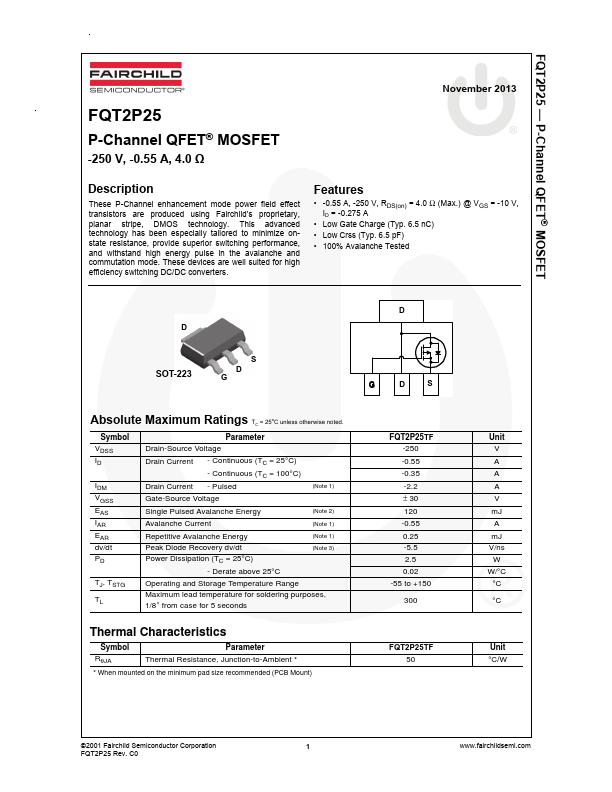
Datasheet4U Logo Datasheet4U.com

FQT2P25 - 250V P-Channel MOSFET

General Description

These P-Channel enhancement mode power field effect transistors are produced using Fairchild’s proprietary, planar stripe, DMOS technology.

Key Features

  • -0.55 A, -250 V, RDS(on) = 4.0 Ω (Max. ) @ VGS = -10 V, ID = -0.275 A.
  • Low Gate Charge (Typ. 6.5 nC).
  • Low Crss (Typ. 6.5 pF).
  • 100% Avalanche Tested D SOT-223 S D G D G D S Absolute Maximum Ratings TC = 25oC unless otherwise noted. Symbol VDSS ID IDM VGSS EAS IAR EAR dv/dt PD TJ, TSTG TL Parameter Drain-Source Voltage Drain Current - Continuous (TC = 25°C) - Continuous (TC = 100°C) Drain Current - Pulsed (Note 1) Gate-Source Voltage Single Pulse.

📥 Download Datasheet

Full PDF Text Transcription (Reference)

The following content is an automatically extracted verbatim text from the original manufacturer datasheet and is provided for reference purposes only.

View original datasheet text
FQT2P25 — P-Channel QFET® MOSFET FQT2P25 P-Channel QFET® MOSFET -250 V, -0.55 A, 4.0 Ω November 2013 Description These P-Channel enhancement mode power field effect transistors are produced using Fairchild’s proprietary, planar stripe, DMOS technology. This advanced technology has been especially tailored to minimize onstate resistance, provide superior switching performance, and withstand high energy pulse in the avalanche and commutation mode. These devices are well suited for high efficiency switching DC/DC converters. Features • -
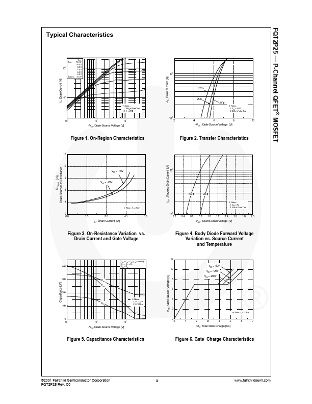
0.55 A, -250 V, RDS(on) = 4.0 Ω (Max.) @ VGS = -10 V, ID = -0.275 A • Low Gate Charge (Typ. 6.5 nC) • Low Crss (Typ. 6.5 pF) • 100% Avalanche Tested D SOT-223 S D G D G D S Absolute Maximum Ratings TC = 25oC unless otherwise noted.