FSA3259
FSA3259 is Dual SP3T Analog Switch manufactured by Fairchild Semiconductor.
Description
The FSA3259 Dual Single Pole Triple Throw (SP3T) analog switch operates from a single 1.65V to 5.5V supply. It features a typical On Resistance (RON) of 9: at a 3.3V supply and 25q C. The device is fabricated with sub-micron CMOS technology to achieve fast switching speeds and is designed for breakbefore-make operation. The FSA3259 also features wide-bandwidth (!250Mbz), high Off Isolation and low crosstalk. The dual SP3T configuration allows for maximum design flexibility.
Features
O 9: typical On Resistance (RON) @ 3.3V O Ideal for 3:1 Multiplex/Demultiplex cell phone applications O Broad VCC operating range: 1.65V to 5.5V O 250MHz
- 3d B Bandwidth O Break-before-make enable circuitry Applications O Cell phone, PDA O Video O Multi-port USB
Ordering Code:
Order Number
FSA3259BQX
Package Number
MLP016E
Package Description
Pb-Free 16-Terminal Depopulated Quad Very-Thin Flat Pack No Leads (DQFN), JEDEC MO-241, 2.5 x 3.5mm
Pb-Free package per JEDEC J-STD-020B. DQFN package available in Tape and Reel only.
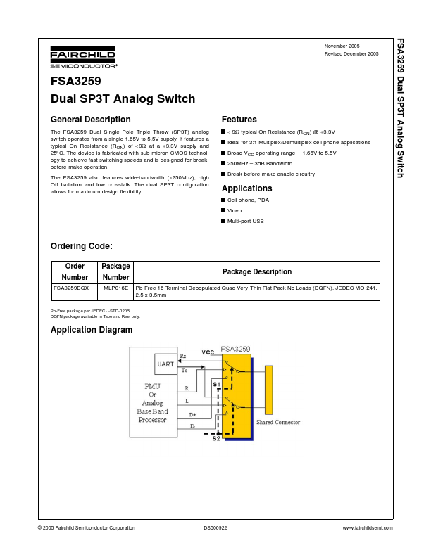
Application Diagram
© 2005 Fairchild Semiconductor Corporation
DS500922
.fairchildsemi.
Analog Symbol
Connection Diagram
(Top Through View)
Pin Descriptions
Pin Name n A, n B0, n B1, n B2 n S1, n S2
Truth Table
Description
Data Ports Control Inputs
Control Inputs (S1, S2) n S1
H = HIGH Logic Level
Function n S2
L L H H No Connection n B0 Connected to n A n B1 Connected to n A n B2 Connected to n A
L = LOW Logic Level
.fairchildsemi.
Absolute Maximum Ratings(Note 1)
Supply Voltage (VCC) Switch Voltage (Note 2) Input Voltage (VIN) (Note 2) Input Diode Current (l IK) Switch Current Peak Switch Current (Pulsed at 1m S Duration, 10% Duty Cycle) Power Dissipation @ 85q C Storage Temperature Range (TSTG) Maximum Junction Temperature (TJ) Lead Temperature (TL) (Soldering, 10 Seconds) ESD Human Body Model I/O to GND 5000V 8000V 150m A TBD
Remended Operating Conditions
(Note 3) Supply Voltage (VCC) Control Input Voltage (VIN)...