H21A
DESCRIPTION
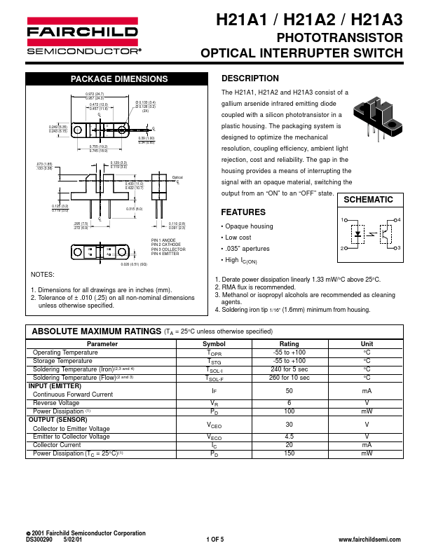
The H21A1, H21A2 and H21A3 consist of a gallium arsenide infrared emitting diode coupled with a silicon phototransistor in a plastic housing. The packaging system is designed to optimize the mechanical resolution, coupling efficiency, ambient light
Ø 0.133 (3.4) Ø 0.126 (3.2) (2X)
C L 0.39 (1.00) 0.34 (0.85)
0.755 (19.2) 0.745 (18.9)
.073 (1.85) .133 (3.38)
0.129 (3.3) 0.119 (3.0) Optical C L rejection, cost and reliability. The gap in the housing provides a means of interrupting the signal with an opaque material, switching the output from an “ON” to an “OFF” state.
0.433 (11.0) 0.422 (10.7)
SCHEMATIC
1 4
0.125 (3.2) 0.119 (3.0) C L .295 (7.5) .272 (6.9)
0.315 (8.0)
FEATURES
0.110 (2.8) 0.091 (2.3)
- Opaque housing
- Low cost
- .035” apertures
- High IC(ON) 1. Derate power dissipation linearly 1.33 m W/°C above 25°C. 2. RMA flux is remended. 3. Methanol or isopropyl alcohols are remended as cleaning agents. 4. Soldering iron tip 1/16” (1.6mm) minimum from...