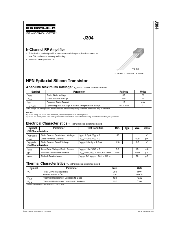
J304 Overview
Key Features
- This device is designed for electronic switching applications such as low ON resistance analog switching
- Sourced from process 50
| Part | J304 |
|---|---|
| Description | N-Channel RF Amplifier |
| Manufacturer | Fairchild Semiconductor |
| Size | 23.69 KB |
| Part Number | Manufacturer | Description |
|---|---|---|
| J304 | InterFET | N-Channel JFET |
| J304 | Vishay | N-Channel JFETs |
| J304 | Motorola Semiconductor | JFET High Frequency Amplifier |
| J304 | Toshiba | 2SJ304 |
| J303 | NEC | 2SJ303 |