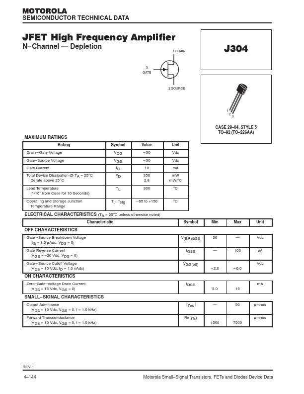
J304 Overview
Key Features
- Gate Voltage
- Source Voltage
| Part | J304 |
|---|---|
| Description | JFET High Frequency Amplifier |
| Manufacturer | Motorola Semiconductor |
| Size | 189.90 KB |
| Part Number | Manufacturer | Description |
|---|---|---|
| J304 | InterFET | N-Channel JFET |
| J304 | Vishay | N-Channel JFETs |
| J304 | Fairchild Semiconductor | N-Channel RF Amplifier |
| J304 | Toshiba | 2SJ304 |
| J303 | NEC | 2SJ303 |