SFH9250L
SFH9250L is Advanced Power MOSFET manufactured by Fairchild Semiconductor.
FEATURES
❑ Logic-Level Gate Drive ❑ Avalanche Rugged Technology ❑ Rugged Gate Oxide Technology ❑ Lower Input Capacitances ❑ Improved Gate Charge ❑ Extended Safe Operating Area ❑ Lower Leakage Current : 10u A (Max.) @ VDS=-200V ❑ Lower RDS(ON) : 0.175 Ω (Typ.)
BVDSS = -200 V RDS(on) = 0.23 Ω ID = -19.5 A
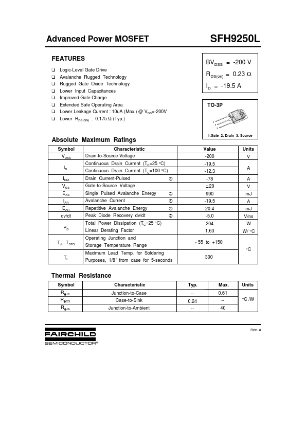
TO-3P
1 2 3
1.Gate 2. Drain 3. Source
Absolute Maximum Ratings
Symbol VDSS ID IDM VGS EAS IAR EAR dv/dt PD TJ , TSTG TL Characteristic Drain-to-Source Voltage Continuous Drain Current (TC=25 °C) Continuous Drain Current (TC=100 °C) Drain Current-Pulsed Gate-to-Source Voltage Single Pulsed Avalanche Energy Avalanche Current Repetitive Avalanche Energy Peak Diode Recovery dv/dt Total Power Dissipation (TC=25 °C) Linear Derating Factor Operating Junction and Storage Temperature Range Maximum Lead Temp. for Soldering Purposes, 1/8″ from case for 5-seconds
② ① ① ③ ①
Value -200 -19.5 -12.3 -78 ±20 990 -19.5 20.4 -5.0 204 1.63
- 55 to +150
Units V A A V m J A m J V/ns W W/ °C
°C 300
Thermal Resistance
Symbol RθJC RθCS RθJA Characteristic Junction-to-Case Case-to-Sink Junction-to-Ambient Typ. -0.24 -Max. 0.61 -40 °C /W Units
Rev. A
Electrical Characteristics (TC=25°C unless otherwise specified)
Symbol BVDSS ΔBV/ΔTJ VGS(th) IGSS IDSS RDS(on) gfs Ciss Coss Crss td(on) tr td(off) tf Qg Qgs Qgd Characteristic Drain-Source Breakdown Voltage Breakdown Voltage Temp. Coeff. Gate Threshold Voltage Gate-Source Leakage , Forward Gate-Source Leakage , Reverse Drain-to-Source Leakage Current Static Drain-Source On-State Resistance Forward Transconductance Input Capacitance Output Capacitance Reverse Transfer Capacitance Turn-On Delay Time Rise Time Turn-Off Delay Time Fall Time Total Gate Charge Gate-Source Charge Gate-Drain(Miller) Charge ------------.175 0.23 13 -Min. Typ. Max. Units -200 --1.0 ------0.17 --------2.0 100 -100 10 100 μA Ω S p F V V n A
P-CHANNEL POWER MOSFET
Test Condition VGS=0V,ID=-250μA See Fig 7 VDS=-5V,ID=-250μA VGS=-20V VGS=20V VDS=-200V...