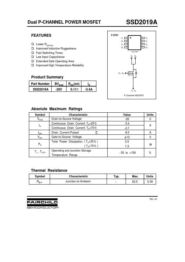
SSD2019A Overview
Key Features
- Improved Inductive Ruggedness !
- Fast Switching Times !
- Low Input Capacitance !
- Extended Safe Operating Area !
| Part | SSD2019A |
|---|---|
| Description | Dual P-Channel Power MOSFET |
| Category | MOSFET |
| Manufacturer | Fairchild Semiconductor |
| Size | 183.45 KB |
| Seller | Inventory | Price Breaks | Buy |
|---|---|---|---|
| UnikeyIC | 400000 | 100+ : 0.1523 USD 200+ : 0.1498 USD 300+ : 0.1459 USD |
View Offer |
| Unikeyic (ICkey) | 400000 | 100+ : 0.1523 USD 200+ : 0.1498 USD 300+ : 0.1459 USD |
View Offer |
| Part Number | Manufacturer | Description |
|---|---|---|
| A2SHB | HAOHAI | N-Channel MOSFET |
| AP9563GH | Advanced Power Electronics Corp | P-CHANNEL ENHANCEMENT MODE POWER MOSFET |
| FCPF360N65S3R0L | onsemi | N-Channel MOSFET |