SSP45N20A
SSP45N20A is advanced power MOSFET manufactured by Fairchild Semiconductor.
FEATURES
Avalanche Rugged Technology Rugged Gate Oxide Technology
..
BVDSS = 200 V RDS(on) = 0.065 Ω ID = 35 A
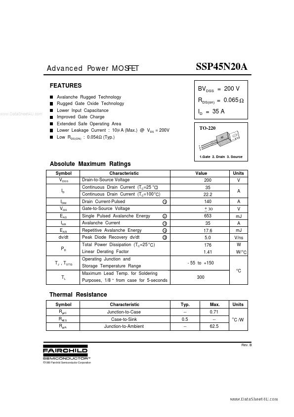
TO-220
Lower Input Capacitance Improved Gate Charge Extended Safe Operating Area Lower Leakage Current : 10 µ A (Max.) @ VDS = 200V Low RDS(ON) : 0.054 Ω (Typ.)
1 2 3
1.Gate 2. Drain 3. Source
Absolute Maximum Ratings
Symbol VDSS ID IDM VGS EAS IAR EAR dv/dt PD TJ , TSTG TL Characteristic Drain-to-Source Voltage Continuous Drain Current (TC=25 C) Continuous Drain Current (TC=100 o C) Drain Current-Pulsed Gate-to-Source Voltage Single Pulsed Avalanche Energy Avalanche Current Repetitive Avalanche Energy Peak Diode Recovery dv/dt Total Power Dissipation (TC=25 o C ) Linear Derating Factor Operating Junction and Storage Temperature Range Maximum Lead Temp. for Soldering Purposes, 1/8 “ from case for 5-seconds
1 O o
Value 200 35 22.2 140 + 30 _ 653 35 17.6 5.0 176 1.41
- 55 to +150
Units V A A V m J A m J V/ns W W/ o C
O 1 O 1 O 3 O
2 o
Thermal Resistance
Symbol RθJC Rθ CS RθJA Characteristic Junction-to-Case Case-to-Sink Junction-to-Ambient Typ. -0.5 -Max. 0.71 -62.5 o
Units
C /W
Rev. B
©1999 Fairchild Semiconductor Corporation
Symbol BVDSS ∆BV/∆ TJ VGS(th)
..
N-CHANNEL POWER MOSFET
Electrical Characteristics (TC=25o C unless otherwise specified)
Characteristic Drain-Source Breakdown Voltage Breakdown Voltage Temp. Coeff. Gate Threshold Voltage Gate-Source Leakage , Forward Gate-Source Leakage , Reverse Drain-to-Source Leakage Current Static Drain-Source On-State Resistance Forward Transconductance Input Capacitance Output Capacitance Reverse Transfer Capacitance Turn-On Delay Time Rise Time Turn-Off Delay Time Fall Time Total Gate Charge Gate-Source Charge Gate-Drain(“ Miller” ) Charge Min. Typ. Max. Units 200 -2.0 -----------------0.21 ------22.83 530 255 22 22 79 36 117 25 48.8 --4.0 100 -100 10 100 0.065 -610 295 60 60 170 80 152 --n C ns µA Ω Ω p F Test Condition VGS=0V ,ID=250µ A V o See Fig 7 V/ C ID=250 µA V n A...