74F273
74F273 is Octal D-Type Flip-Flop manufactured by Fairchild Semiconductor.
Description
The 74F273 has eight edge-triggered D-type flip-flops with individual D inputs and Q outputs. The mon buffered Clock (CP) and Master Reset (MR) inputs load and reset (clear) all flip-flops simultaneously. The register is fully edge-triggered. The state of each D input, one setup time before the LOW-to-HIGH clock transition, is transferred to the corresponding flip-flop’s Q output. All outputs will be forced LOW independently of Clock or Data inputs by a LOW voltage level on the MR input. The device is useful for applications where the true output only is required and the Clock and Master Reset are mon to all storage elements.
Features s Ideal buffer for MOS microprocessor or memory s Eight edge-triggered D-type flip-flops s Buffered mon clock s Buffered, asynchronous Master Reset s See 74F377 for clock enable version s See 74F373 for transparent latch version s See 74F374 for 3-STATE version
Ordering Code:
Order Number 74F273SC 74F273SJ 74F273PC Package Number M20B M20D N20A Package Description
20-Lead Small Outline Integrated Circuit (SOIC), JEDEC MS-013, 0.300 Wide 20-Lead Small Outline Package (SOP), EIAJ TYPE II, 5.3mm Wide 20-Lead Plastic Dual-In-Line Package (PDIP), JEDEC MS-001, 0.300 Wide
Devices also available in Tape and Reel. Specify by appending the suffix letter “X” to the ordering code.
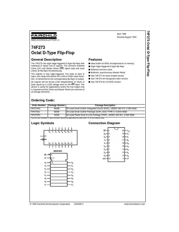
Logic Symbols
Connection Diagram
IEEE/IEC
© 1999 Fairchild Semiconductor Corporation
DS009511
.fairchildsemi.
Unit Loading/Fan Out
U.L. Pin Names D0- D7 MR CP Q0- Q7 Data Inputs Master Reset (Active LOW) Clock Pulse Input (Active Rising Edge) Data Outputs Description
HIGH/LOW 1.0/1.0 1.0/1.0 1.0/1.0 50/33.3 Input IIH/IIL Output IOH/IOL 20 µA/- 0.6 m A 20 µA/- 0.6 m A 20 µA/- 0.6 m A
- 1 m A/20 m A
Mode Select-Function Table
Inputs Operating Mode MR Reset (Clear) Load “1” Load “0” L H H CP Dn X h l Output Qn L H L
H = HIGH Voltage Level steady state h = HIGH Voltage Level one setup time prior to the LOW-to-HIGH clock transition L = LOW...