NDP6030
NDP6030 is P-Channel Logic Level Enhancement Mode Field Effect Transistor manufactured by Fairchild Semiconductor.
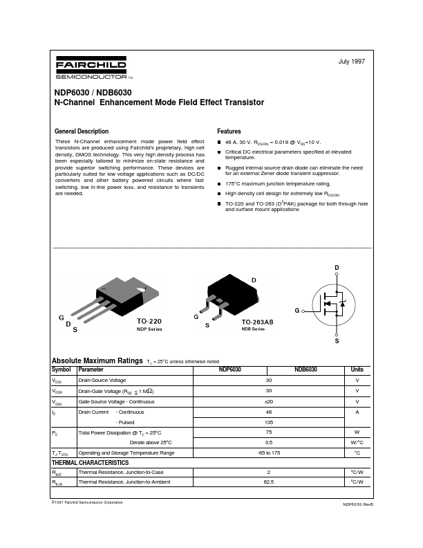
Description
These N-Channel enhancement mode power field effect transistors are produced using Fairchild's proprietary, high cell density, DMOS technology. This very high density process has been especially tailored to minimize on-state resistance and provide superior switching performance. These devices are particularly suited for low voltage applications such as DC/DC converters and other battery powered circuits where fast switching, low in-line power loss, and resistance to transients are needed.
Features
46 A, 30 V. RDS(ON) = 0.018 @ VGS=10 V. Critical DC electrical parameters specified at elevated temperature. Rugged internal source-drain diode can eliminate the need for an external Zener diode transient suppressor. 175°C maximum junction temperature rating. High density cell design for extremely low RDS(ON). TO-220 and TO-263 (D2PAK) package for both through hole and surface mount applications
Absolute Maximum Ratings
Symbol VDSS VDGR VGSS ID Parameter Drain-Source Voltage
T C = 25°C unless otherwise noted
NDP6030 30 30 ±20 46 135 75 0.5 -65 to 175
NDB6030
Units V V V A
Drain-Gate Voltage (RGS < 1 MΩ) Gate-Source Voltage
- Continuous Drain Current
- Continuous
- Pulsed
Total Power Dissipation @ TC = 25°C Derate above 25°C
W W/°C °C
TJ,TSTG RθJC Rθ JA
Operating and Storage Temperature Range
THERMAL CHARACTERISTICS Thermal Resistance, Junction-to-Case Thermal Resistance, Junction-to-Ambient 2 62.5 °C/W °C/W
© 1997 Fairchild Semiconductor Corporation
NDP6030.Rev B
Electrical Characteristics (TC = 25°C unless otherwise noted)
Symbol Parameter Conditions Min Typ Max Units DRAIN-SOURCE AVALANCHE RATINGS (Note) W DSS IAR BVDSS Single Pulse Drain-Source Avalanche Energy Maximum Drain-Source Avalanche Current VDD = 15 V, ID = 46 A 100 46 m J A
OFF CHARACTERISTICS Drain-Source Breakdown Voltage Breakdown Voltage Temp. Coefficient Zero Gate Voltage Drain Current...