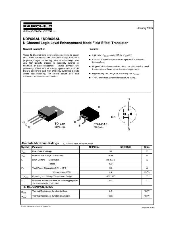
NDP603AL
NDP603AL is N-Channel Logic Level Enhancement Mode Field Effect Transistor manufactured by Fairchild Semiconductor.
Description
These N-Channel logic level enhancement mode power field effect transistors are produced using Fairchild's proprietary, high cell density, DMOS technology. This very high density process is especially tailored to minimize on-state resistance. These devices are particularly suited for low voltage applications such as DC/DC converters and high efficiency switching circuits where fast switching, low in-line power loss, and resistance to transients are needed.
Features
25A, 30V. RDS(ON) = 0.022Ω @ VGS=10V. Critical DC electrical parameters specified at elevated temperature. Rugged internal source-drain diode can eliminate the need for an external Zener diode transient suppressor. High density cell design for extremely low RDS(ON). 175°C maximum junction temperature rating.
Absolute Maximum Ratings
Symbol VDSS VGSS ID Parameter Drain-Source Voltage
T C = 25°C unless otherwise noted
NDP603AL 30 ± 20 25
(Note 1)
NDB603AL
Units V V A
Gate-Source Voltage
- Continuous Drain Current
- Continuous
- Pulsed
100 50 0.4 -65 to 175 275 W W/°C °C °C
Total Power Dissipation @ TC = 25°C Derate above 25°C
TJ,TSTG TL
Operating and Storage Temperature Range Maximum lead temperature for soldering purposes, 1/8" from case for 5 seconds
THERMAL CHARACTERISTICS RθJC RθJA Thermal Resistance, Junction-to-Case Thermal Resistance, Junction-to-Ambient 2.5 62.5 °C/W °C/W
© 1997 Fairchild Semiconductor Corporation
NDP603AL.SAM
Electrical Characteristics (TC = 25°C unless otherwise noted)
Symbol Parameter Conditions Min Typ Max Units DRAIN-SOURCE AVALANCHE RATINGS (Note 2) W DSS IAR BVDSS IDSS IGSSF IGSSR VGS(th) Single Pulse Drain-Source Avalanche Energy Maximum Drain-Source Avalanche Current VDD = 15 V, ID = 25 A 100 25 m J A
OFF CHARACTERISTICS Drain-Source Breakdown Voltage Zero Gate Voltage Drain Current Gate
- Body Leakage, Forward Gate
- Body Leakage, Reverse VGS = 0 V, ID =...