FEATURES
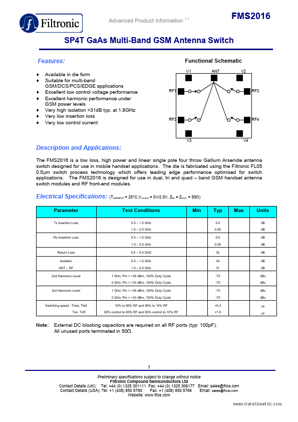
: ♦ ♦ ♦ ♦ ♦ ♦ ♦ Available in die form Suitable for multi-band GSM/DCS/PCS/EDGE applications Excellent low control voltage performance Excellent harmonic performance under GSM power levels Very high isolation >31dB typ. at 1.8GHz Very low insertion loss Very low control current Functional Schematic V1 ANT V2 RF1 RF2 RF3 RF4 V3 V4 DESCRIPTION
and APPLICATIONS
: ELECTRICAL SPECIFICATIONS
: Parameter Tx Insertion Loss (TAMBIENT = 25°C,Vcontrol = 0V/2.5V, ZIN = ZOUT = 50Ω) Test Conditions 0.5 – 1.0 GHz 1.0 – 2.0 GHz Min Typ 0.5 0.55 0.5 0.55 32 34 31 -75 -75 -75 -75 <0.3 <1.0 Max Units dB dB dB dB dB dB dB dBc dBc dBc dBc µs µs Rx Insertion Loss 0.5 – 1.0 GHz 1.0 – 2.0 GHz Return Loss Isolation ANT – RF 2nd Harmonic Level 0.5 – 2.5 GHZ 0.5 – 1.0 GHz 1.0 – 2.0 GHz 1 GHz, Pin = +35 dBm, 100% Duty Cycle 2 GHz, Pin = +33 dBm, 100% Duty Cycle 3rd Harmonic Level 1 GHz, Pin = +35 dBm, 100% Duty Cycle 2 GHz, Pin = +33 dBm, 100% Duty Cycle Switching speed : Trise, Tfall Ton, Toff 10% to 90% RF and 90% to 10% RF 50% control to 90% RF and 50% control to 10% RF Note: External DC blocking capacitors are required on all RF ports (typ: 100pF). Filtronic