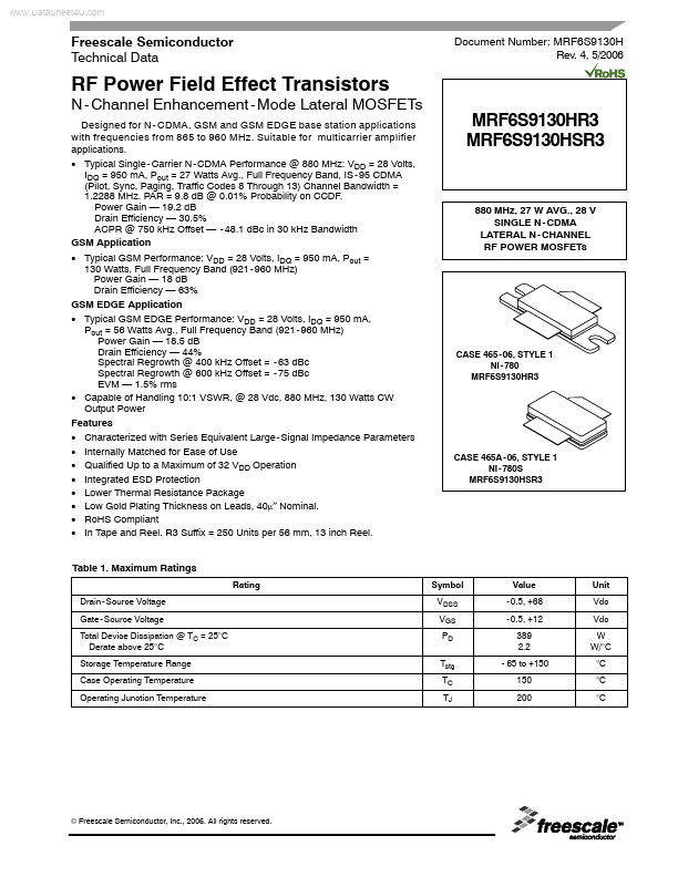
MRF6S9130HSR3
MRF6S9130HSR3 is RF Power Field Effect Transistors manufactured by Freescale Semiconductor.
- Part of the MRF6S9130HR3 comparator family.
- Part of the MRF6S9130HR3 comparator family.
..
Freescale Semiconductor Technical Data
Document Number: MRF6S9130H Rev. 4, 5/2006
RF Power Field Effect Transistors
- Channel Enhancement
- Mode Lateral MOSFETs
Designed for N
- CDMA, GSM and GSM EDGE base station applications with frequencies from 865 to 960 MHz. Suitable for multicarrier amplifier applications.
- Typical Single
- Carrier N
- CDMA Performance @ 880 MHz: VDD = 28 Volts, IDQ = 950 m A, Pout = 27 Watts Avg., Full Frequency Band, IS
- 95 CDMA (Pilot, Sync, Paging, Traffic Codes 8 Through 13) Channel Bandwidth = 1.2288 MHz. PAR = 9.8 d B @ 0.01% Probability on CCDF. Power Gain
- 19.2 d B Drain Efficiency
- 30.5% ACPR @ 750 k Hz Offset
- - 48.1 d Bc in 30 k Hz Bandwidth GSM Application
- Typical GSM Performance: VDD = 28 Volts, IDQ = 950 m A, Pout = 130 Watts, Full Frequency Band (921
- 960 MHz) Power Gain
- 18 d B Drain Efficiency
- 63% GSM EDGE Application
- Typical GSM EDGE Performance: VDD = 28 Volts, IDQ = 950 m A, Pout = 56 Watts Avg., Full Frequency Band (921
- 960 MHz) Power Gain
- 18.5 d B Drain Efficiency
- 44% Spectral Regrowth @ 400 k Hz Offset =
- 63 d Bc Spectral Regrowth @ 600 k Hz Offset =
- 75 d Bc EVM
- 1.5% rms
- Capable of Handling 10:1 VSWR, @ 28 Vdc, 880 MHz, 130 Watts CW Output Power Features
- Characterized with Series Equivalent Large
- Signal Impedance Parameters
- Internally Matched for Ease of...