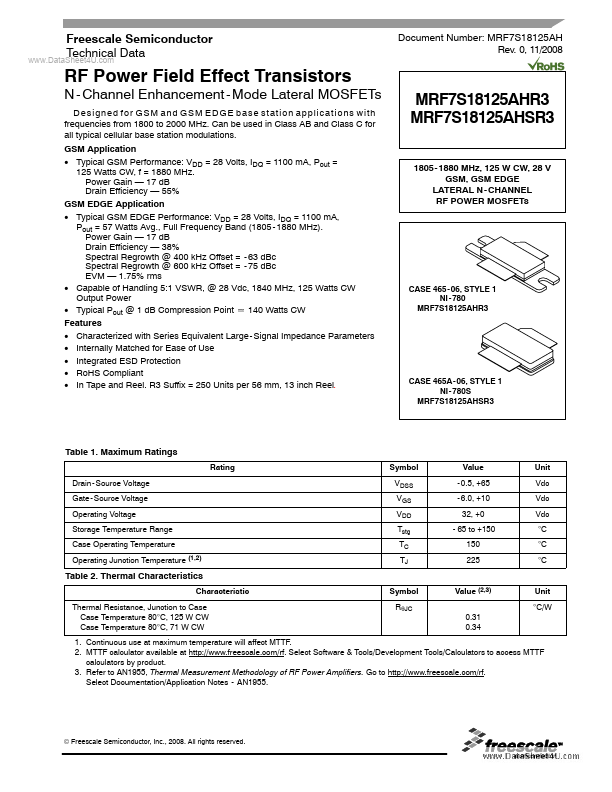
Datasheet4U Logo Datasheet4U.com

MRF7S18125AHSR3 - RF Power Field Effect Transistors

This page provides the datasheet information for the MRF7S18125AHSR3, a member of the MRF7S18125AHR3 RF Power Field Effect Transistors family.

Description

1 μF, 50 V Chip Capacitor 4.7 μF, 50 V Chip Capacitors 220 μF, 63 V Electrolytic Chip Capacitor 8.2 pF Chip Capacitors 0.2 pF Chip Capacitors 0.5 pF Chip Capacitor 10 kΩ, 1/4 W Chip Resistors 10 Ω, 1/4 W Chip Resistor Part Number C3216X5R1H105K C4532X5R1H475M 2222 136 68221 ATC100B8R2BT500XT ATC100B

Features

  • Characterized with Series Equivalent Large - Signal Impedance Parameters.
  • Internally Matched for Ease of Use.
  • Integrated ESD Protection.
  • RoHS Compliant.
  • In Tape and Reel. R3 Suffix = 250 Units per 56 mm, 13 inch Reel. MRF7S18125AHR3 MRF7S18125AHSR3 1805- 1880 MHz, 125 W CW, 28 V GSM, GSM EDGE.

📥 Download Datasheet

Datasheet preview – MRF7S18125AHSR3

Datasheet Details

Part number MRF7S18125AHSR3
Manufacturer Freescale Semiconductor
File Size 511.61 KB
Description RF Power Field Effect Transistors
Datasheet download datasheet MRF7S18125AHSR3 Datasheet
Additional preview pages of the MRF7S18125AHSR3 datasheet.
Other Datasheets by Freescale Semiconductor

Full PDF Text Transcription

Click to expand full text
Freescale Semiconductor Technical Data www.DataSheet4U.com Document Number: MRF7S18125AH Rev. 0, 11/2008 RF Power Field Effect Transistors N - Channel Enhancement - Mode Lateral MOSFETs Designed for GSM and GSM EDGE base station applications with frequencies from 1800 to 2000 MHz. Can be used in Class AB and Class C for all typical cellular base station modulations. GSM Application • Typical GSM Performance: VDD = 28 Volts, IDQ = 1100 mA, Pout = 125 Watts CW, f = 1880 MHz. Power Gain — 17 dB Drain Efficiency — 55% GSM EDGE Application • Typical GSM EDGE Performance: VDD = 28 Volts, IDQ = 1100 mA, Pout = 57 Watts Avg., Full Frequency Band (1805 - 1880 MHz).
Published: |