Datasheet4U Logo Datasheet4U.com

MRF7S21170HSR3 - RF Power Field Effect Transistors

This page provides the datasheet information for the MRF7S21170HSR3, a member of the MRF7S21170HR3 RF Power Field Effect Transistors family.

Features

  • 100% PAR Tested for Guaranteed Output Power Capability.
  • Characterized with Series Equivalent Large--Signal Impedance Parameters.
  • Internally Matched for Ease of Use.
  • Integrated ESD Protection.
  • Greater Negative Gate--Source Voltage Range for Improved Class C Operation.
  • Optimized for Doherty.

📥 Download Datasheet

Datasheet preview – MRF7S21170HSR3

Datasheet Details

Part number MRF7S21170HSR3
Manufacturer Freescale Semiconductor
File Size 507.95 KB
Description RF Power Field Effect Transistors
Datasheet download datasheet MRF7S21170HSR3 Datasheet
Additional preview pages of the MRF7S21170HSR3 datasheet.
Other Datasheets by Freescale Semiconductor

Full PDF Text Transcription

Click to expand full text
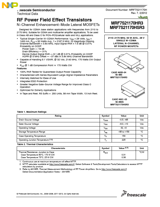
Freescale Semiconductor Technical Data RF Power Field Effect Transistors N--Channel Enhancement--Mode Lateral MOSFETs Designed for CDMA base station applications with frequencies from 2110 to 2170 MHz. Suitable for CDMA and multicarrier amplifier applications. To be used in Class AB and Class C for PCN--PCS/cellular radio and WLL applications.  Typical Single--Carrier W--CDMA 1C4h0a0nnmeAl ,BPanoudtw=id5t0h Watts Avg., f = 3.84 MHz, =Pe2r1fo6r7m.5anMcHe:z,VIDQDM=a2g8nVituodltes,CIDliQpp=ing, Input Signal PAR = 7.5 dB @ 0.01% Probability on CCDF. Power Gain — 16 dB Drain Efficiency — 31% Device Output Signal PAR — 6.1 dB @ 0.01% Probability on CCDF ACPR @ 5 MHz Offset — --37 dBc in 3.
Published: |