MB85R256
MB85R256 is Memory FRAM manufactured by Fuji Electric.
FEATURES
- -
- -
- -
- Bit configuration: 32,768 words x 8 bits Read/write durability: 1010 times/bit (Min) Peripheral circuit CMOS construction Operating power supply voltage: 3.0 V to 3.6 V Operating temperature range:
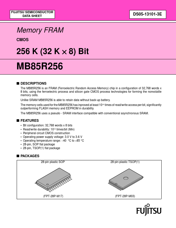
- 40 °C to +85 °C 28-pin, SOP flat package 28-pin, TSOP(1) flat package s PACKAGES
28-pin plastic SOP 28-pin plastic TSOP(1)
(FPT-28P-M17)
(FPT-28P-M03)
MB85R256 s PIN ASSIGNMENTS
(TOP VIEW)
A14 A12 A7 A6 A5 A4 A3 A2 A1 A0 I/O0 I/O1 I/O2 GND
1 2 3 4 5 6 7 8 9 10 11 12 13 14
28 27 26 25 24 23 22 21 20 19 18 17 16 15
VCC WE A13 A8 A9 A11 OE A10 CE I/O7 I/O6 I/O5 I/O4 I/O3 OE A11 A9 A8 A13 WE VCC A14 A12 A7 A6 A5 A4 A3 22 23 24 25 26 27 28 1 2 3 4 5 6 7 21 20 19 18 17 16 15 14 13 12 11 10 9 8 A10 CE I/O7 I/O6 I/O5 I/O4 I/O3 GND I/O2 I/O1 I/O0 A0 A1 A2
(FPT-28P-M17)
(FPT-28P-M03) s PIN DESCRIPTIONS
Pin name A0 to A14 I/O0 to I/O7 CE WE OE VCC GND Address Input Data input/output Chip enable input Write Enable input Output enable input Power supply ( + 3.3 V Typ) Ground Function
MB85R256 s BLOCK DIAGRAM
A14 to A10
Block decoder
A14 to A0
Address latch
A7 to A0
Row decoder
FRAM array: 32,768 x 8
Pseudo-SRAM interface logic circuit
A8, A9
Column decoder
Control logic I/O latch bus driver
I/O0-I/O7 I/O7 to I/O0
OE s FUNCTION LIST
Operation mode Standby precharge Latch address Write Read Output Disable CE H × L L L × L H H H L H WE × L OE × L I/O7 to I/O0 High-Z Data input Data output High-Z Operation (ICC) Power supply current Standby (ISB)
H: High level, L: Low level, x: Irrespective of “H” or “L”
MB85R256 s ABSOLUTE MAXIMUM RANGES
Parameter Power supply voltage Input voltage Output voltage Operating temperature Storage temperature Symbol VCC VIN VOUT TA Tstg Rating...