MB84VD2109x Description
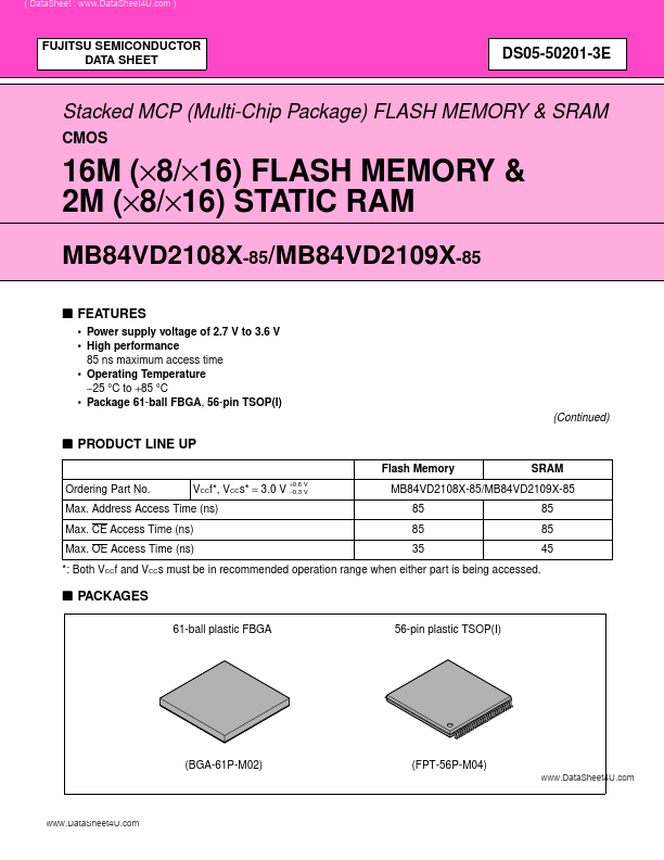
( DataSheet : .. ) FUJITSU SEMICONDUCTOR DATA SHEET DS05-50201-3E Stacked MCP (Multi-Chip Package) FLASH MEMORY & SRAM CMOS 16M (×8/×16) FLASH MEMORY & 2M (×8/×16) STATIC RAM MB84VD2108X-85/MB84VD2109X-85.
MB84VD2109x Key Features
- Power supply voltage of 2.7 V to 3.6 V
- High performance 85 ns maximum access time
- Operating Temperature -25 °C to +85 °C
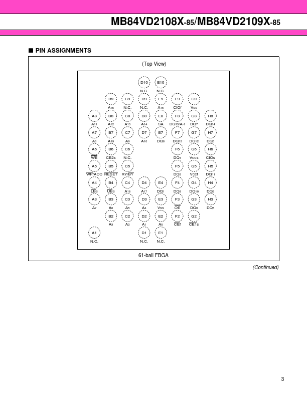
- Package 61-ball FBGA, 56-pin TSOP(I)
- Both VCCf and VCCs must be in remended operation range when either part is being accessed
- Simultaneous Read/Write operations (dual bank) Multiple devices available with different bank sizes Host system can prog
- Minimum 100,000 write/erase cycles
- Sector erase architecture Eight 4 K words and thirty one 32 K words. Any bination of sectors can be concurrently erased.
- Boot Code Sector Architecture MB84VD2108X : Top sector MB84VD2109X : Bottom sector
- Embedded EraseTM- Algorithms Automatically pre-programs and erases the chip or any sector