MB84VD23381EF Description
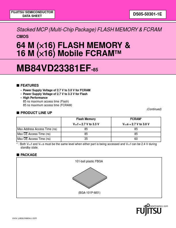
) FUJITSU SEMICONDUCTOR DATA SHEET DS05-50301-1E Stacked MCP (Multi-Chip Package) FLASH MEMORY & FCRAM CMOS 64 M (×16) FLASH MEMORY & 16 M (×16) Mobile FCRAMTM MB84VD23381EF-85.
MB84VD23381EF Key Features
- Power Supply Voltage of 2.7 V to 3.0 V for FCRAM
- Power Supply Voltage of 2.7 V to 3.3 V for Flash
- High Performance 85 ns maximum access time (Flash) 85 ns maximum access time (FCRAM)
- Both VCCf and VCCs must be the same level when either part is being accessed and VCCf can be 2.4 V during standby state
- Operating Temperature -30 °C to +85 °C
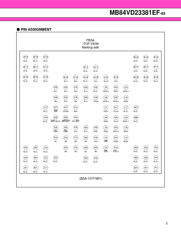
- Package 101-ball FBGA
- FLASH MEMORY
- Simultaneous Read/Write Operations (FlexBankTM) Two virtual Banks are chosen from the bination of four physical banks Ho
- Minimum 100,000 Write/Erase Cycles
- Sector Erase Architecture Sixteen 4 K words and one hundred twenty-six 32 K word sectors. Any bination of sectors can be