MBM29SL800BE
Key Features
- 0.23 µm Process Technology
- Single 1.8 V read, program, and erase Minimizes system level power requirements
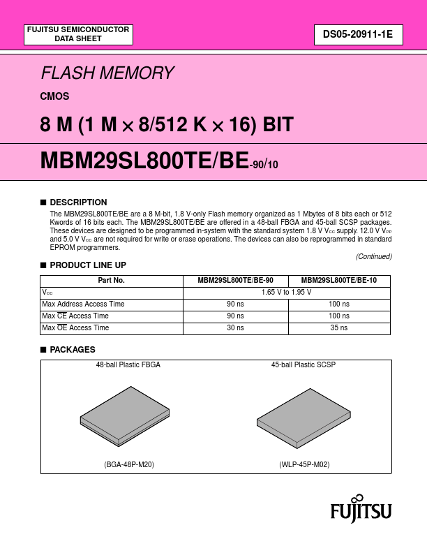
- compatible with JEDEC-standard world-wide pinouts 48-ball FBGA (Package suffix : PBT) 45-ball SCSP (Package suffix : PW)
- Minimum 100,000 program/erase cycles
- High performance 90 ns maximum access time
- Sector erase architecture One 8 Kword, two 4 Kwords, one 16 Kword, and fifteen 32 Kwords se