FLL357ME
FLL357ME is L-band Medium & High Power GAAS Fets manufactured by Fujitsu Semiconductor Limited.
FEATURES
- -
- -
- High Output Power: P1d B=35.5d Bm (Typ.) High Gain: G1d B=11.5d B (Typ.) High PAE: ηadd=46% (Typ.) Proven Reliability Hermetically Sealed Package
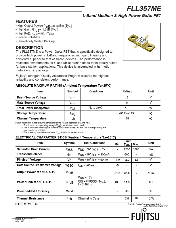
DESCRIPTION
The FLL357ME is a Power Ga As FET that is specifically designed to provide high power at L-Band frequencies with gain, linearity and efficiency superior to that of silicon devices. The performance in multitone environments for Class AB operation make them ideally suited for base station applications. This device is assembled in hermetic metal/ceramic package. Fujitsu’s stringent Quality Assurance Program assures the highest reliability and consistent performance. ABSOLUTE MAXIMUM RATING (Ambient Temperature Ta=25°C)
Item Drain-Source Voltage Gate-Source Voltage Total Power Dissipation Storage Temperature Channel Temperature Symbol VDS VGS Ptot Tstg Tch Tc = 25°C Condition Rating 15 -5 15 -65 to +175 175 Unit V V W °C °C
Fujitsu remends the following conditions for the reliable operation of Ga As FETs: 1. The drain-source operating voltage (VDS) should not exceed 10 volts. 2. The forward and reverse gate currents should not exceed 19.4 and -2.0 m A respectively with gate resistance of 100Ω. 3. The operating channel temperature (Tch) should not exceed 145°C.
ELECTRICAL CHARACTERISTICS (Ambient Temperature Ta=25°C)
Item Saturated Drain Current Transconductance Pinch-off Voltage Gate Source Breakdown Voltage Output Power at 1d B G.C.P. Symbol IDSS gm Vp VGSO P1d B G1d B ηadd Rth Channel to Case VDS = 10V IDS ≈ 0.6IDSS (Typ.), f = 2.3GHz Test Conditions VDS = 5V, VGS = 0V VDS = 5V, IDS = 800m A VDS = 5V, IDS = 60m A IGS = -60µA Min. -1.0 -5 34.5 10.5 Limit Typ. Max. 1200 1800 600 -2.0 35.5 11.5 46 7.5 -3.5 10 Unit m A m S V V d Bm d B % °C/W
Power Gain at 1d B G.C.P. Power-added Efficiency Thermal Resistance CASE STYLE: ME
G.C.P.: Gain pression Point ..
.. Edition 1.1
July 1999
L-Band Medium & High Power Ga As FET
POWER DERATING CURVE 16 Total Power Dissipation (W) VGS =0V -0.5V 800 -1.0V 400...