Fujitsu MB85R1002
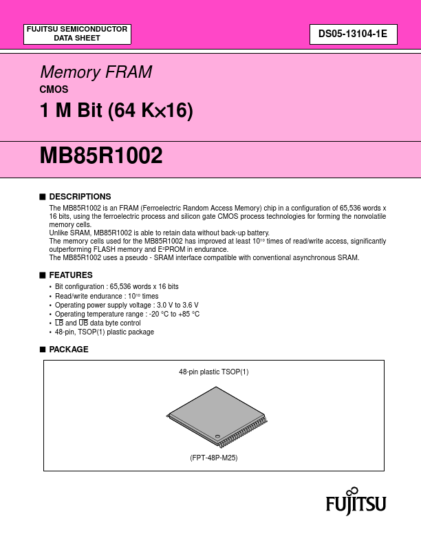
The MB85R1002 is an FRAM (Ferroelectric Random Access Memory) chip in a configuration of 65,536 words x 16 bits, using the ferroelectric process and silicon gate CMOS process technologies for forming the nonvolatile memory cells. The memory cells used for the MB85R1002 has improved at least 1010 times of read/write access, significantly outperforming FLASH memory and E2PROM in endurance. The MB85R1002 uses a pseudo - SRAM interface compatible with conventional asynchronous SRAM.| Part No. | MB85R1002 |
|---|---|
| Datasheet | MB85R1002 Download |
| Manufacturer |  Fujitsu |
| Description | Memory FRAM |
| Buy | Stock & Price |
FEATURES
●●
●
●
●
● Bit configuration : 65,536 words x 16 bits Read/write endurance : 1010 times Operating power supply voltage : 3.0 V to 3.6 V Operating temperature range : -20 °C to +85 °C LB and UB data byte control 48-pin, TSOP(1) plastic package
● PACKAGE 48-pin plastic TSOP(1) (FPT-48P-M25) MB85R1002
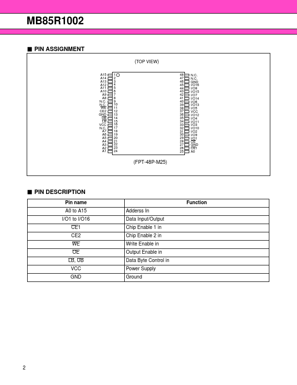
● PIN ASSIGNMENT (TOP VIEW) A15 A14 A13 A12 A11 A10 A9 A8 N.C. N.C. WE CE2 GND UB LB VCC N.C. A7 A6 A5 A4 A3 A2 A1 1 2 3 4 5 6 7 8 9 10 11 12 13 14 15 16 17 18 19 20 21 22 23 24 48 47 46 45 44 43 42 41 40 39 38 37 36 35 34 33 32 31 30 29 28 27 26 25 N.C. N.C. GND I/O16 I/O8 I/O15 I/O7 I/O14 I/O6 I/O13 I/O5 VCC I/O12 I/O4 I/O11 I/O3 I/O10 I/O2 I/O9 I/O1 OE GND CE1 A0 (FPT-48P-M25)
● PIN
DESCRIPTION
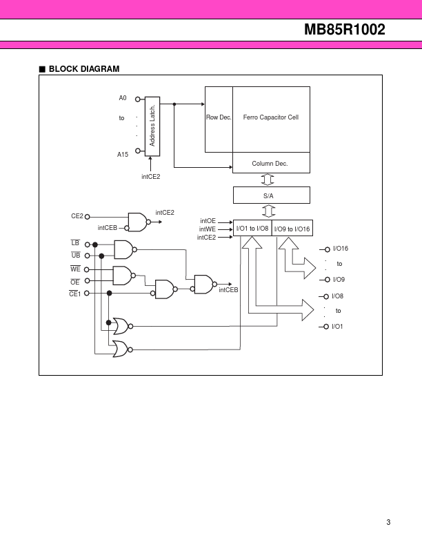
Pin name A0 to A15 I/O1 to I/O16 CE1 CE2 WE OE LB, UB VCC GND Adderss In Data Input/Output Chip Enable 1 in Chip Enable 2 in Write Enable in Output Enable in Data Byte Control in Power Supply Ground Function 2 MB85R1002● BLOCK DIAGRAM A0 to
●
●
● Address Latch. Row Dec. Ferro Capacitor C...