GS8161E18DGT
Features
- FT pin for user-configurable flow through or pipeline operation
- Dual Cycle Deselect (DCD) operation
- IEEE 1149.1 JTAG-patible Boundary Scan
- 2.5 V or 3.3 V +10%/- 10% core power supply
- 2.5 V or 3.3 V I/O supply
- LBO pin for Linear or Interleaved Burst mode
- Internal input resistors on mode pins allow floating mode pins
- Default to Interleaved Pipeline mode
- Byte Write (BW) and/or Global Write (GW) operation
- Internal self-timed write cycle
- Automatic power-down for portable applications
- JEDEC-standard 165-bump BGA package
- Ro HS-pliant 100-pin TQFP and 165-bump BGA available
Functional Description
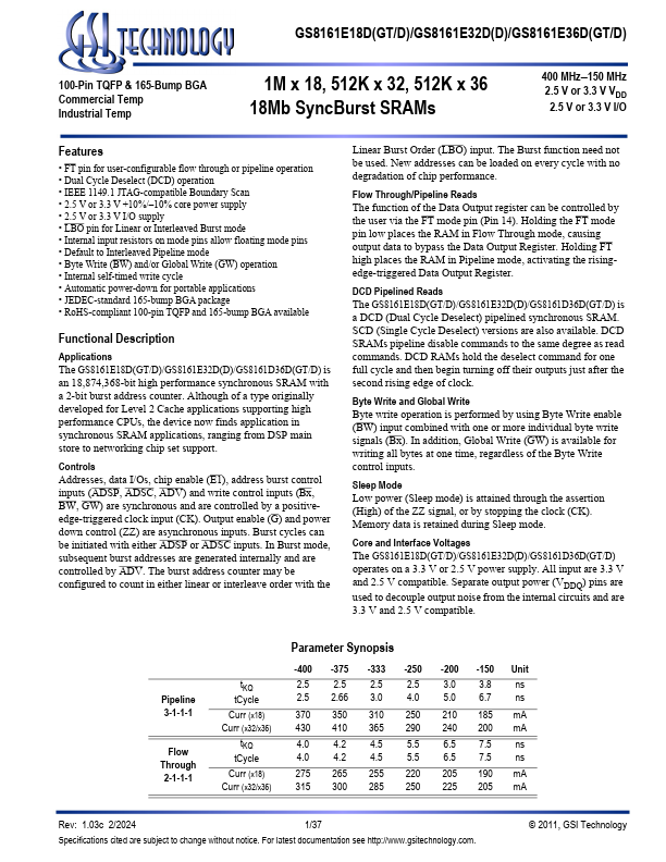
Applications The GS8161E18D(GT/D)/GS8161E32D(D)/GS8161D36D(GT/D) is an 18,874,368-bit high performance synchronous SRAM with a 2-bit burst address counter. Although of a type originally developed for Level 2 Cache applications supporting high performance CPUs, the device now finds application in synchronous SRAM applications, ranging from DSP main store to networking...