GS8170DD18C-300
GS8170DD18C-300 is SigmaRAM SRAM manufactured by GSI Technology.
- Part of the GS8170DD18C comparator family.
- Part of the GS8170DD18C comparator family.
Preliminary GS8170DD18/36C-333/300/250
209-Bump BGA mercial Temp Industrial Temp
18Mb Σ1x2Lp Double Data Rate Sigma RAM™ SRAM
250 MHz- 333 MHz 1.8 V VDD 1.8 V and 1.5 V I/O
Features
- Double Data Rate Read and Write mode
- JEDEC-standard Sigma RAM™ pinout and package
- 1.8 V +150/- 100 m V core power supply
- 1.5 V or 1.8 V I/O supply
- Pipelined read operation
- Fully coherent read and write pipelines
- Echo Clock outputs track data output drivers
- ZQ mode pin for user-selectable output drive strength
- 2 user-programmable chip enable inputs for easy depth expansion
- IEEE 1149.1 JTAG-patible Boundary Scan
- 209-bump, 14 mm x 22 mm, 1 mm bump pitch BGA package
- Pin-patible with future 36Mb, 72Mb, and 144Mb devices
- 333 3.0 ns 1.6 ns
Pipeline mode t KHKH t KHQV
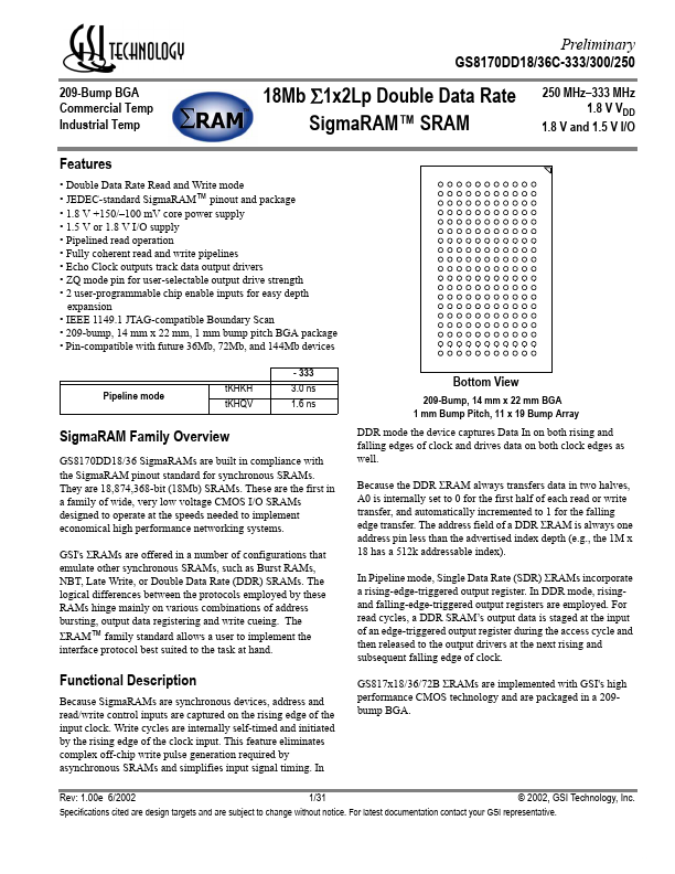
Bottom View
209-Bump, 14 mm x 22 mm BGA 1 mm Bump Pitch, 11 x 19 Bump Array DDR mode the device captures Data In on both rising and falling edges of clock and drives data on both clock edges as well. Because the DDR ΣRAM always transfers data in two halves, A0 is internally set to 0 for the first half of each read or write transfer, and automatically incremented to 1 for the falling edge transfer. The address field of a DDR ΣRAM is always one address pin less than the advertised index depth (e.g., the 1M x 18 has a 512k addressable index). In Pipeline mode, Single Data Rate (SDR) ΣRAMs incorporate a rising-edge-triggered output register. In DDR mode, risingand falling-edge-triggered output registers are employed. For read cycles, a DDR SRAM’s output data is staged at the input of an edge-triggered output register during the access cycle and then released to the output drivers at the next rising and subsequent falling edge of clock. GS817x18/36/72B ΣRAMs are implemented with GSI's high performance CMOS technology and are packaged in a 209bump BGA.
Sigma RAM Family Overview
GS8170DD18/36 Sigma RAMs are built in pliance with the Sigma RAM pinout standard for synchronous SRAMs. They are...