GSI Technology GS8330LW36C
This feature eliminates complex off-chip write pulse generation required by asynchronous SRAMs and simplifies input signal timing. They also utilize a Dual Cycle Deselect (DCD) output deselect protocol.| Part No. | GS8330LW36C |
|---|---|
| Datasheet | GS8330LW36C Download |
| Manufacturer |  GSI Technology |
| Description | 36Mb 1x1Lp CMOS I/O Late Write SigmaRAM |
| Buy | Stock & Price |
FEATURES
● Late Write mode, Pipelined Read mode● JEDEC-standard SigmaRAM™ pinout and package
● 1.8 V +150/–100 mV core power supply
● 1.8 V CMOS Interface
● ZQ controlled user-selectable output drive strength
● Dual Cycle Deselect
● Burst Read and Write option
● Fully coherent read and write pipelines
● Echo Clock outputs track data output drivers
● Byte write operation (9-bit bytes)
● 2 user-programmable chip enable inputs
● IEEE 1149.1 JTAG-compliant Serial Boundary Scan
● 209-bump, 14 mm x 22 mm, 1 mm bump pitch BGA package
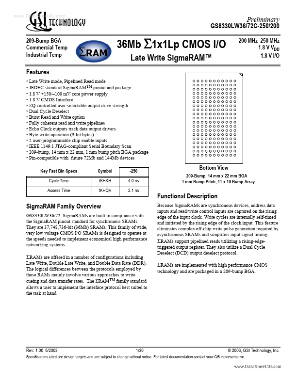
● Pin-compatible with future 72Mb and 144Mb devices Key Fast Bin Specs Cycle Time Access Time Symbol tKHKH tKHQV -250 4.0 ns 2.1 ns Bottom View 209-Bump, 14 mm x 22 mm BGA 1 mm Bump Pitch, 11 x 19 Bump Array Functional
DESCRIPTION
Because SigmaRAMs are synchronous devices, address data inputs and read/write control inputs are captured on the rising edge of the input clock. Write cycles are internally self-timed and initiated by the rising edge of the clock input. ΣRAMs support pipelined reads utilizing a rising-edgetriggered output register.
