
GS88118B Overview
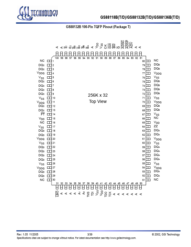
Applications The GS88118B(T/D)/GS88132B(T/D)/GS88136B(T/D) is a 9,437,184-bit high performance synchronous SRAM with a 2bit burst address counter. Although of a type originally developed for Level 2 Cache applications supporting high performance CPUs, the device now finds application in synchronous SRAM applications, ranging from DSP main store to networking chip set support. Controls Addresses, data I/Os, chip...
GS88118B Key Features
- IEEE 1149.1 JTAG-patible Boundary Scan
- 2.5 V or 3.3 V +10%/-10% core power supply
- 2.5 V or 3.3 V I/O supply
- LBO pin for Linear or Interleaved Burst mode
- Internal input resistors on mode pins allow floating mode pins
- Byte Write (BW) and/or Global Write (GW) operation
- Internal self-timed write cycle
- Automatic power-down for portable