GI405
GI405 is P-CHANNEL ENHANCEMENT MODE POWER MOSFET manufactured by GTM.
Description
The GI405 uses advanced trench technology to provide excellent on-resistance, low gate charge and low gate resistance. The through-hole version (TO-251) is available for low-profile applications and suited for high current load applications.
- Simple Drive Requirement
- Lower On-resistance
- Fast Switching Characteristic
Features
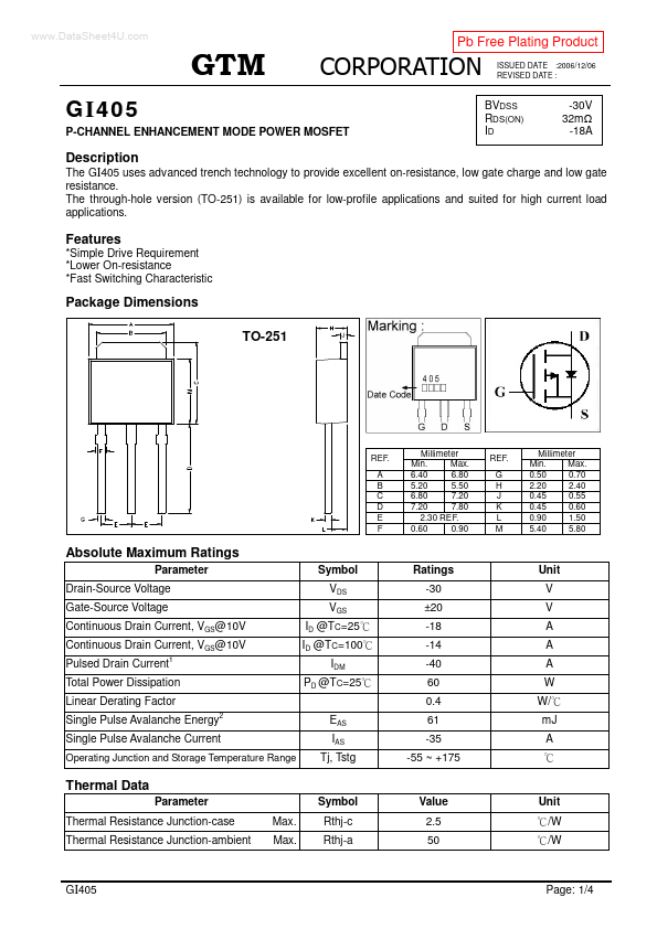
Package Dimensions TO-251
REF. A B C D E F
Millimeter Min. Max. 6.40 6.80 5.20 5.50 6.80 7.20 7.20 7.80 2.30 REF. 0.60 0.90
REF. G H J K L M
Millimeter Min. Max. 0.50 0.70 2.20 2.40 0.45 0.55 0.45 0.60 0.90 1.50 5.40 5.80
Absolute Maximum Ratings
Parameter Drain-Source Voltage Gate-Source Voltage Continuous Drain Current, VGS@10V Continuous Drain Current, VGS@10V Pulsed Drain Current
Symbol VDS VGS ID @TC=25 ID @TC=100 IDM PD @TC=25
Ratings -30 ±20 -18 -14 -40 60 0.4 61 -35 -55 ~ +175
Unit V V A A A W W/ m J A
Total Power Dissipation Linear Derating Factor Single Pulse Avalanche Energy
EAS IAS Tj, Tstg
Single Pulse Avalanche Current
Operating Junction and Storage Temperature Range
Thermal Data
Parameter Thermal Resistance Junction-case Thermal Resistance Junction-ambient Max. Max. Symbol Rthj-c Rthj-a Value 2.5 50 Unit /W /W
Page: 1/4
ISSUED DATE :2006/12/06 REVISED DATE :
Electrical Characteristics (Tj = 25
Parameter Drain-Source Breakdown Voltage Gate Threshold Voltage Forward Transconductance Gate-Source Leakage Current
Drain-Source Leakage Current(Tj=25 ) Drain-Source Leakage Current(Tj=55 ) unless otherwise specified)
Min. -30 -1.2 Typ. 17 18.7 2.54 5.4 9 25 20 12 920 190 122 Max. -2.4 ±100 -1 -5 32 60 23 13 1100 p F ns n C Unit V V S n A u A u A m Test Conditions VGS=0, ID=-250u A VDS=VGS, ID=-250u A VDS=-5V, ID=-18A VGS= ±20V VDS=-30V, VGS=0 VDS=-24V, VGS=0 VGS=-10V, ID=-18A VGS=-4.5V, ID=-10A ID=-18A VDS=-15V VGS=-10V VDS=-15V VGS=-10V RG=3 RL=0.82 VGS=0V VDS=-15V f=1.0MHz
Symbol BVDSS VGS(th) gfs IGSS IDSS
Static Drain-Source On-Resistance3 Total Gate Charge3 Gate-Source Charge Gate-Drain...