GI88LS02
GI88LS02 is N-CHANNEL ENHANCEMENT MODE POWER MOSFET manufactured by GTM.
..
Pb Free Plating Product
ISSUED DATE :2006/01/05 REVISED DATE :
Description
N-CHANNEL ENHANCEMENT MODE POWER MOSFET
BVDSS RDS(ON) ID
25V 5m 75A
The GI88LS02 used advanced design and process to achieve low gate charge, low on-resistance and fast switching performance. The through-hole version (TO-251) is available for low-profile applications and suited for low voltage applications such as DC/DC converters.
- Low Gate Charge
- Simple Drive Requirement
- Fast Switching
Features
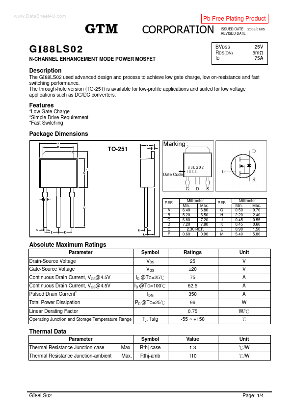
Package Dimensions TO-251
REF. A B C D E F
Millimeter Min. Max. 6.40 6.80 5.20 5.50 6.80 7.20 7.20 7.80 2.30 REF. 0.60 0.90
REF. G H J K L M
Millimeter Min. Max. 0.50 0.70 2.20...