HM30P03Q
Features
- VDSS=-30V/VGSS=±20V/ID=-30A RDS(ON)=14mΩ(max.)@VGS=-10V RDS(ON)=22mΩ(max.)@VGS=-4.5V
- Low Dense Cell Design
- Reliable and Rugged
- Advanced trench process technology
Applications z Synchronous Rectification z Power Management in Inverter System
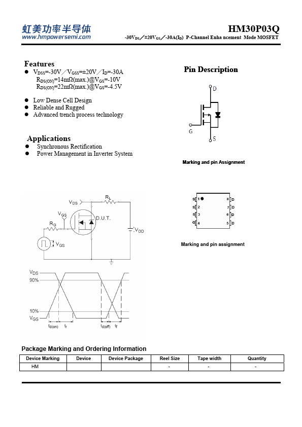
Pin Description
Marking and pin Assignment
Markin g and pin assignment
Package Marking and Ordering Information
Device Marking
Device
Device Package
HM34 +034 ')1;/
Reel Size
- Tape width
- Quantity
-
-30VDS/±20VGS/-30A(ID) P-Channel Enha ncement Mode MOSFET
Electrical Characteristics of CP Test (TA=25°C unless otherwise noted)
Symbol
Parameter
Test Conditions
Static Characteristics
BVDSS Drain-Source Breakdown Voltage VGS=0V,ID=-250u A
IDSS
Zero Gate Voltage Drain Current
VDS=-24V,VGS=0V TJ=85°C
VGS(th) Gate Threshold Voltage
VDS=VGS,ID=-250u A
IGSS Gate Leakage Current
VGS=±20V,...