HM80N70
HM80N70 is N-Channel Enhancement Mode Power MOSFET manufactured by H&M Semiconductor.
+01
80VDS/±25VGS/66A(ID) N-Channel Enha ncement Mode MOSFET
Features
- VDSS=80V/VGSS=±25V/ID=66A RDS(ON)=12mΩ(Max.)@VGS=10V
- Reliab le and Rugged
- Advancedtrench process technology
- High Density Cell Design For Ultra Low On-Resistance
Applications
- Synchronous Rectification - Power Management in Inverter System
Switching Time Test Circuit and Waveforms
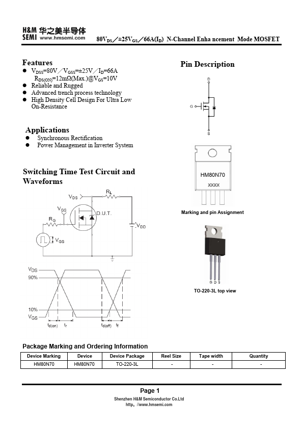
Pin Description
Marking and pin Assignment
TO-220-3L top view
Package Marking and Ordering Information
Device Marking HM80N70
Device HM80N70
Device Package TO-220-3L
Reel Size
- Page 1
Shenzhen H&M Semiconductor Co.Ltd http://.hmsemi.
Tape width
- Quantity
- +01
80VDS/±25VGS/66A(ID) N-Channel Enha ncement Mode...