HT741A Overview
Key Features
- Large input voltage range
- Short-circuit protection
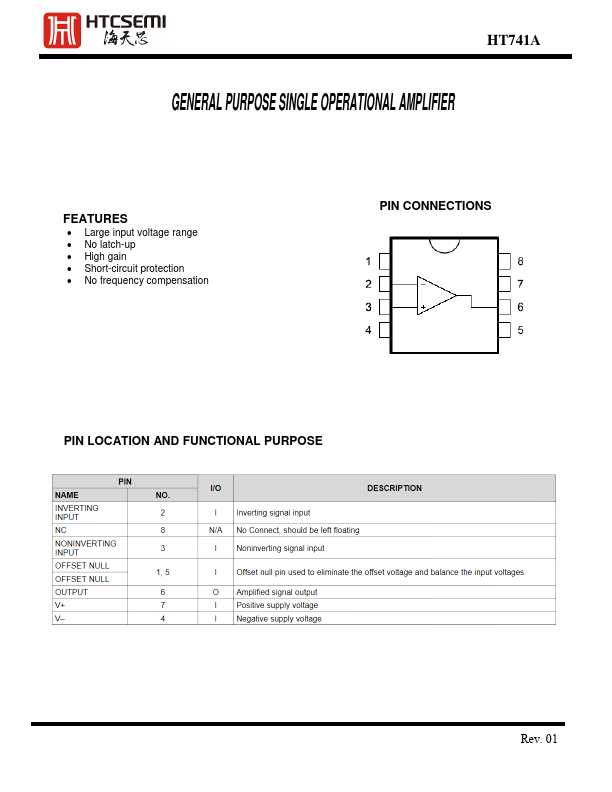
- No frequency compensation PIN LOCATION AND FUNCTIONAL PURPOSE Rev. 01 HT741A Rev. 01 HT741A
| Part | HT741A |
|---|---|
| Description | GENERAL PURPOSE SINGLE OPERATIONAL AMPLIFIER |
| Category | Operational Amplifier |
| Manufacturer | HTCSEMI |
| Size | 321.12 KB |
| Seller | Inventory | Price Breaks | Buy |
|---|---|---|---|
| LCSC | 50 | 5+ : 0.2931 USD 50+ : 0.2122 USD 150+ : 0.1873 USD 500+ : 0.1563 USD |
View Offer |
| Part Number | Manufacturer | Description |
|---|---|---|
| HT74173 | Holtek Semiconductor | 6.0V 3.0A 1.2MHz Synchronous Step-Down Converter |
| HT74153 | Holtek Semiconductor | 6.0V 2.0A 1.2MHz Synchronous Step-Down Converter |
| HT74164 | Holtek Semiconductor | 8-Bit Serial-In/Parallel-Out Shift Register |
| HT7463A | Holtek Semiconductor | Asynchronous Step Down Converter |
| HT7463B | Holtek Semiconductor | Asynchronous Step Down Converter |