HMF1M32M8S
HMF1M32M8S is FLASH-ROM MODULE manufactured by Hanbit Electronics.
DESCRIPTION
The HMF1M32M8S is a high-speed flash read only memory (FROM) module containing 1,048,576 words organized in a x32bit configuration. The module consists of eight 512K x 8 FROM mounted on a 72 -pin, both-sided, FR4-printed circuit board.In order to write control, the HMF1M32M8S provides Write Enable and Write Disable selection by SMT switch. mands are written to the mand register using standard microprocessor write timings. Register contents serve as input to an internal state-machine, which controls the erase and programming circuitry. Write cycles also internally latch addresses and data needed for the programming and erase operations. Reading data out of the
.. device is similar to reading from 12.0V flash or EPROM devices. Eight chip enable inputs, (/CE-UU1, /CE_UM1, /CE_LM1,
/CE_LL1, /CE_UU2, /CE_UM2, /CE_LM2, /CE_LL2) are used to enable the module ’s 4 bytes independently. Output enable (/OE) and write enable (/WE) can set the memory input and output .. When FROM module is disable condition the module is being power standby mode, system designer can get low -power design. All module ponents may be powered from a single +5V DC power supply and all inputs and outputs are TTL patible
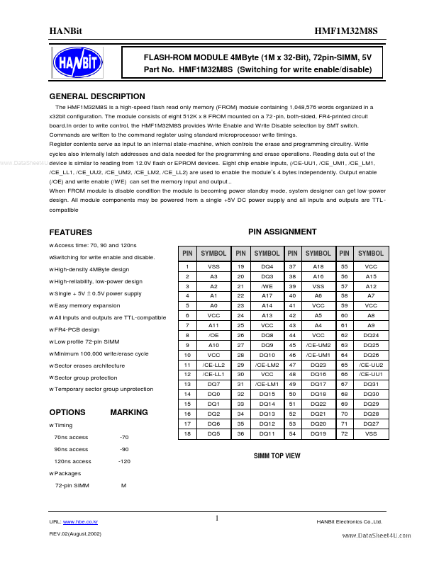
Features w Access time: 70, 90 and 120ns w Switching for write enable and disable. w High-density 4MByte design w High-reliability, low-power design w Single + 5V ± 0.5V power supply w Easy memory expansion w All inputs and outputs are TTL-patible w FR4-PCB design w Low profile 72-pin SIMM w Minimum 100,000 write/erase cycle w Sector erases architecture w Sector group protection w Temporary sector group unprotection PIN 1 2 3 4 5 6 7 8 9 10 11 12 13 14 15 16 17 -70 -90 -120 18 SYMBOL VSS A3 A2 A1 A0 VCC A11 /OE A10 VCC /CE-LL2 /CE-LL1 DQ7 DQ0 DQ1 DQ2 DQ6 DQ5 PIN 19 20 21 22 23 24 25 26 27 28 29 30 31 32 33 34 35 36
PIN ASSIGNMENT
SYMBOL DQ4 DQ3 /WE A17 A14 A13 VCC DQ8 DQ9 DQ10 /CE-LM2 VCC /CE-LM1 DQ15 DQ14 DQ13 DQ12 DQ11 PIN 37 38 39 40 41 42 43 44 45 46 47 48 49 50 51...