GENERAL DESCRIPTION
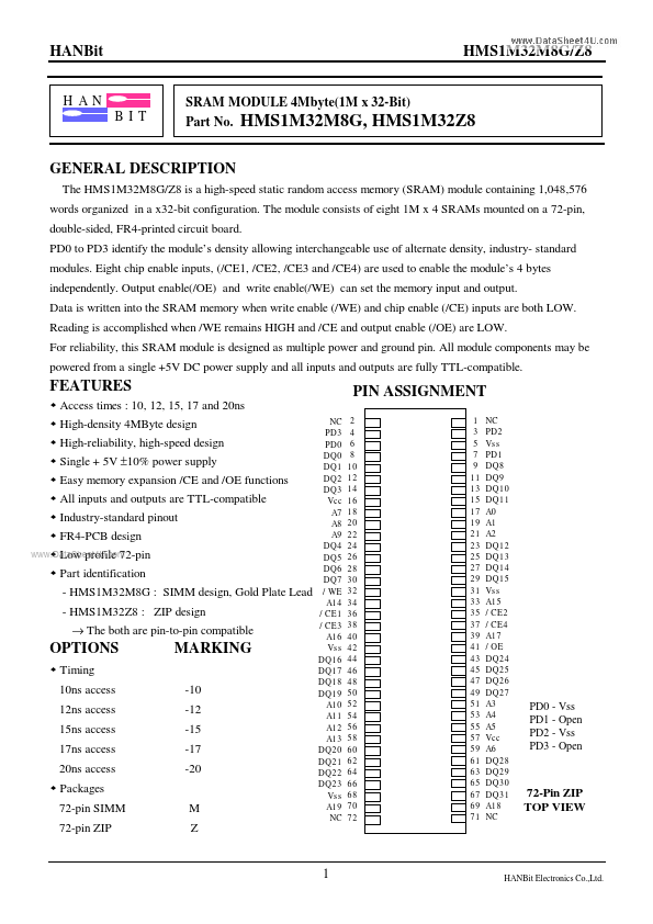
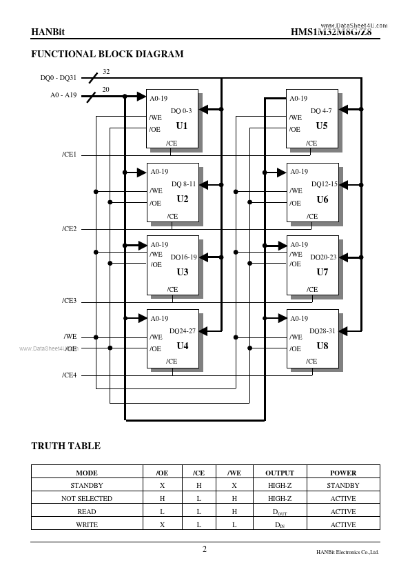
PD0 to PD3 identify the module’s density allowing interchangeable use of alternate density, industry- standard modules. Eight chip enable inputs, (/CE1, /CE2, /CE3 and /CE4) are used to enable the module’s 4 bytes independently. Output enable(/OE) and write enable(/WE) can set the memory input and output. Data is written into the SRAM memory when write enable (/WE) and chip enable (/CE) inputs are both LOW. Reading is accomplished when /WE remains HIGH and /CE and output enable (/OE) are LOW. For reliability, this SRAM module is designed as multiple power and ground pin. All module components may be powered from a single +5V DC power supply and all inputs and outputs are fully TTL-compatible. FEATURES
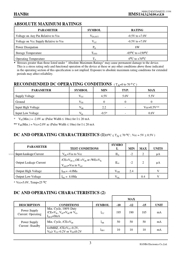
Access times : 10, 12, 15, 17 and 20ns High-density 4MByte design High-reliability, high-speed design Single + 5V ±10% power supply Easy memory expansion /CE and /OE functions All inputs and outputs are TTL-compatible Industry-standard pinout FR4-PCB de... Hanbit Electronics