2SD1366A
2SD1366A is Silicon NPN Transistor manufactured by Hitachi Semiconductor.
Silicon NPN Epitaxial
Application
Low frequency power amplifier
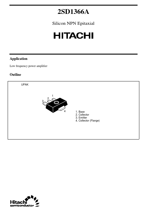
Outline
UPAK
1 3 2
1. Base 2. Collector 3. Emitter 4. Collector (Flange)
Absolute Maximum Ratings (Ta = 25°C)
Item Collector to base voltage Collector to emitter voltage Emitter to base voltage Collector current Collector peak current Collector power dissipation Junction temperature Storage temperature Symbol VCBO VCEO VEBO IC i C(peak)- PC
- Tj Tstg
2 1
Ratings 30 25 5 1 1.5 1 150
- 55 to +150
Unit V V V A A W °C °C
Notes: 1. PW ≤ 10 ms, Duty cycle ≤ 20%. 2. Value on the alumina ceramic board (12.5 × 20 × 0.7 mm)
Electrical Characteristics (Ta = 25°C)
Item Collector to base breakdown voltage Symbol V(BR)CBO Min 30 25 5
- -
Typ
- -
- -
Max
- -
- 0.1 0.1
Unit V V V µA µA
Test conditions I C = 10 µA, IE = 0 I C = 1 m A, RBE = ∞ I E = 10 µA, IC = 0 VCB = 20 V, IE = 0 VEB = 4 V, IC = 0 VCE = 2 V, IC = 0.5 A, Pulse
Collector to emitter breakdown V(BR)CEO voltage Emitter to base breakdown voltage Collector cutoff current Emitter cutoff current DC current transfer ratio Collector to emitter saturation voltage Base to emitter saturation voltage Gain bandwidth product Collector output capacitance Note: Mark h FE AC 85 to 170 AD 120 to 240 V(BR)EBO I CBO I EBO h FE-
- -
- -
- 0.15 0.9 240 22
240 0.3 1.0
- - V V MHz p F
VCE(sat) VBE(sat) f T Cob
I C = 0.8 A, IB = 0.08 A, Pulse I C = 0.8 A, IB = 0.08 A, Pulse VCE = 2 V, IC = 0.5 A, Pulse VCB = 10 V, IE = 0, f = 1 MHz
1. The 2SD1366A is grouped by h FE as follows.
See characteristic curves of 2SD1366.
Maximum Collector Dissipation Curve Collector Power Dissipation PC (W) (on the alumina ceramic board)...