The following content is an automatically extracted verbatim text
from the original manufacturer datasheet and is provided for reference purposes only.
View original datasheet text
2SJ181(L), 2SJ181(S)
Silicon P-Channel MOS FET
Application
High speed power switching
Features
• • • • • Low on-resistance High speed switching Low drive current No secondary breakdown Suitable for switching regulator and DC-DC converter
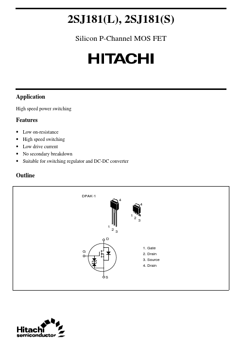
Outline
DPAK-1 4 4 1 1 D G 1. Gate 2. Drain 3. Source 4. Drain S
2
3
2 3
2SJ181(L), 2SJ181(S)
Absolute Maximum Ratings (Ta = 25°C)
Item Drain to source voltage Gate to source voltage Drain current Drain peak current Body to drain diode reverse drain current Channel dissipation Channel temperature Storage temperature Notes: 1. PW ≤ 10 µs, duty cycle ≤ 1% 2. Value at TC = 25°C Symbol VDSS VGSS ID I D(pulse)* I DR Pch* Tch Tstg
2 1
Ratings –600 ±15 –0.5 –1.0 –0.