2SJ181
2SJ181 is Silicon P-Channel MOS FET manufactured by Hitachi Semiconductor.
- Part of the 2SJ182 comparator family.
- Part of the 2SJ182 comparator family.
( DataSheet : .. )
2SJ181(L), 2SJ181(S)
Silicon P-Channel MOS FET
Application
High speed power switching
Features
- -
- -
- Low on-resistance High speed switching Low drive current No secondary breakdown Suitable for switching regulator and DC-DC converter
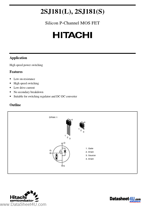
Outline
DPAK-1 4 4 1 1 D G 1. Gate 2. Drain 3. Source 4. Drain S
2 3
..
2SJ181(L),...