2SJ399
Overview
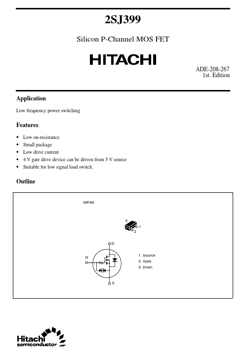
- Low on-resistance Small package Low drive current 4 V gate drive device can be driven from 5 V source Suitable for low signal load switch. Outline MPAK 3 1 2 *
- Source
- Drain G S 2SJ399
| Part | 2SJ399 |
|---|---|
| Description | P-Channel MOSFET |
| Category | MOSFET |
| Manufacturer | Hitachi Semiconductor |
| Size | 36.97 KB |
| Part Number | Manufacturer | Description |
|---|---|---|
| 2SJ399 | Renesas | Silicon P-Channel MOSFET |