The following content is an automatically extracted verbatim text
from the original manufacturer datasheet and is provided for reference purposes only.
View original datasheet text
2SJ451
Silicon P-Channel MOS FET
ADE-208-382 1st. Edition
Application
Low frequency power switching
Features
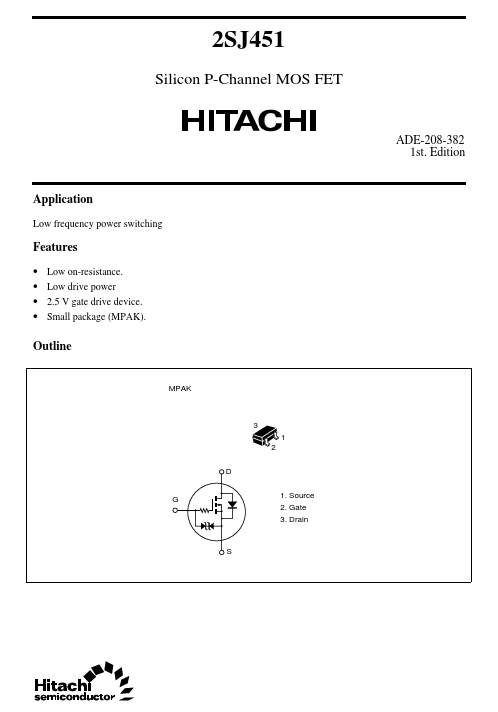
• • • • Low on-resistance. Low drive power 2.5 V gate drive device. Small package (MPAK).
Outline
MPAK
3 1 2 D 1. Source 2. Gate 3. Drain
G
S
2SJ451
Absolute Maximum Ratings (Ta = 25°C)
Item Drain to source voltage Gate to source voltage Drain current Drain peak current Channel dissipation Channel temperature Storage temperature Note: 1. PW ≤ 10 µs, duty cycle ≤ 1% Marking is "ZK–". Symbol VDSS VGSS ID I D(pulse)* Pch Tch Tstg
1
Ratings –20 ±20 –0.2 –0.4 150 150 –55 to +150
Unit V V A A mW °C °C
Electrical Characteristics (Ta = 25°C)
Item Drain to source breakdown voltage Gate to source breakdown voltage Symbol V(BR)DSS V(BR)GSS Min –20 ±20 — — –0.5 — — 0.