The following content is an automatically extracted verbatim text
from the original manufacturer datasheet and is provided for reference purposes only.
View original datasheet text
2SK322
Silicon N-Channel Junction FET
Application
HF wide band amplifier
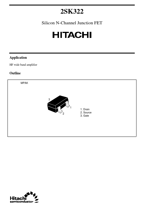
Outline
MPAK
3 1 2
1. Drain 2. Source 3. Gate
2SK322
Absolute Maximum Ratings (Ta = 25°C)
Item Gate to drain voltage Gate to source voltage Drain current Gate current Channel power dissipation Channel temperature Storage temperature Symbol VGDO VGSO ID IG Pch Tch Tstg Ratings –15 –15 50 5 150 150 –55 to +150 Unit V V mA mA mW °C °C
Electrical Characteristics (Ta = 25°C)
Item Gate to drain breakdown voltage Gate to source breakdown voltage Gate cutoff current Drain current Gate to source cutoff voltage Forward transfer admittance Note: Grade Mark I DSS P WP 5 to 16 Q WQ 14 to 24 Symbol V(BR)GDO V(BR)GSO I GSS I DSS*
1
Min –15 –15 — 5 — 25 R WR
Typ — — — — — 45 S
Max — — –10 50 –3.