3SK317
Features
- Low noise characteristics; (NF = 1.0 d B typ. at f = 200 MHz)
- High power gain characteristics ; (PG = 27.6 d B typ. at f = 200 MHz)
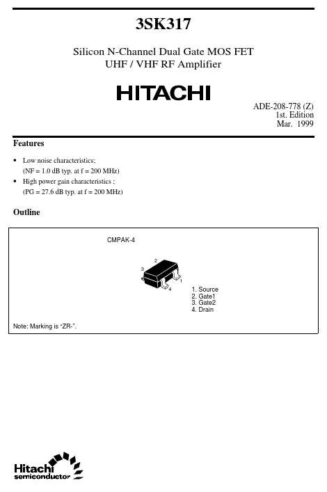
Outline
CMPAK-4
2 3 1 4
1. Source 2. Gate1 3. Gate2 4. Drain
Note: Marking is “ZR-”.
Absolute Maximum Ratings (Ta = 25°C)
Item Drain to source voltage Gate1 to source voltage Gate2 to source voltage Drain current Channel power dissipation Channel temperature Storage temperature Symbol VDS VG1S VG2S ID Pch Tch Tstg Ratings 14 ±8 ±8 25 100 150
- 55 to +150 Unit V V V m A m W °C °C
Electrical Characteristics (Ta = 25°C)
Item Symbol Min 14 ±8 ±8
- - 0 0 4 20 2.4 0.8
- 24
- 12
- - Typ
- -
- -
- 0.2 0.3 8 25 3.1 1.1 0.021 27.6 1.0 15.6 3 2.7 Max
- -
- ±100 ±100 1 1 14
- 3.5 1.4 0.04
- 1.5
- 4 3.5 Unit V V V n A n A V V m A m S p F p F p F d B d B d B d B d B VDS = 6 V, VG2S = 3 V I D = 10 m A , f = 200 MHz VDS = 6 V, VG2S = 3 V I D = 10 m A , f = 900 MHz VDS = 6 V, VG2S = 3 V I D = 10 m A , f = 60 MHz Test Conditions I D = 200 µA VG1S = VG2S = -3 V I G1 =...