HVD142
HVD142 is Silicon Epitaxial Planar Pin Diode manufactured by Hitachi Semiconductor.
Silicon Epitaxial Planar Pin Diode for Antenna Switching
ADE-208-1117 (Z) Rev.0 Jan. 2001 Features
- Low capacitance. (C = 0.35 p F max)
- Low forward resistance. (rf=1.5 Ω max)
- Super small Flat Package (SFP) is suitable for surface mount design.
Ordering Information
Type No. HVD142 Laser Mark T2 Package Code SFP
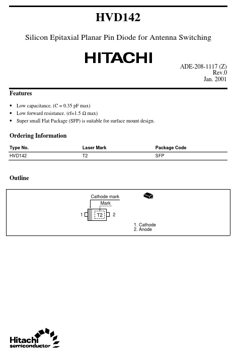
Outline
Cathode mark Mark 1
T2
2 1. Cathode 2....