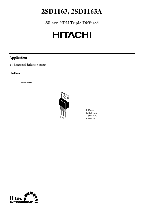
Hitachi 2SD1163
NPN TRANSISTOR
| Part No. | 2SD1163 |
|---|---|
| Datasheet | 2SD1163 Download |
| Manufacturer |  Hitachi |
| Description | NPN TRANSISTOR |
| Buy | Stock & Price |
ABSOLUTE MAXIMUM RATINGS
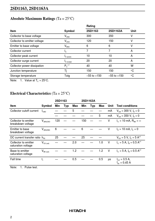
(Ta = 25°C) Rating Item Collector to base voltage Collector to emitter voltage Emitter to base voltage Collector current Collector peak current Collector surge current Collector power dissipation Junction temperature Storage temperature Note: 1. Value at TC = 25°C. Symbol VCBO VCEO VEBO IC I C (peak) I C (surge) PC * Tj Tstg 1 2SD1163 300 120 6 7 10 20 40 150 –55 to +150 2SD1163A 350 150 6 7 10 20 40 150 –55 to +150 Unit V V V A A A W °C °CELECTRICAL CHARACTERISTICS
(Ta = 25°C) 2SD1163 Item Collector cutoff current Symbol I CBO Min — — Collector to emitter breakdown voltage Emitter to base breakdown voltage V(BR)CEO V(BR)EBO 120 6 25 — — — Typ — — — — — — — — Max 5 — — — — 2.0 1.2 0.5 2SD1163A Min — — 150 6 25 — — — Typ — — — — — — — — Max — 5 — — — 1.0 1.2 0.5 V V µs Unit mA mA V V Test conditions VCB = 300 V, IE = 0 VCB = 350 V, IE = 0 I C = 10 mA, RBE = ∞ I E = 10 mA, IC = 0 VCE = 5 V, IC = 5 A*1 I C = 5 A, IB = 0.5 A*1 I C = 5 A, IB = 0.5 A*1 I CP = 3.5 A, I B1 = 0.45 A DC current transfer ratio hFE Collector to emitter saturation voltage Base to emitter saturation voltage Fall time Note: 1.